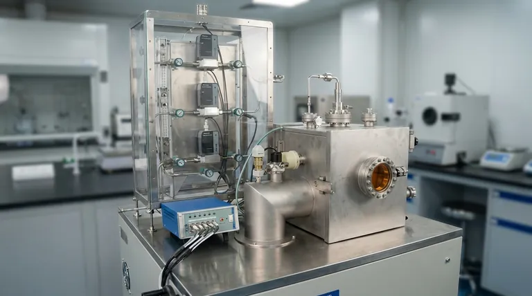
At its core, Plasma-Enhanced Chemical Vapor Deposition (PECVD) offers a unique combination of low-temperature processing, superior film quality, and precise control over material properties. Unlike traditional methods that rely solely on high heat, PECVD uses an energized plasma to drive the chemical reaction, allowing for the deposition of highly uniform and durable thin films onto a wide variety of materials without causing thermal damage.
The fundamental advantage of PECVD is its ability to decouple the energy required for deposition from the temperature of the substrate. This makes it an indispensable tool for fabricating advanced materials on heat-sensitive components, from flexible electronics to complex optical devices.
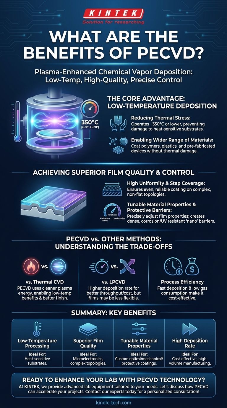
The Core Advantage: Low-Temperature Deposition
The most significant benefit of PECVD is its ability to operate at much lower temperatures than conventional Chemical Vapor Deposition (CVD), typically around 350°C or even lower. This is possible because the energy needed to initiate the chemical reaction comes from a plasma field, not just thermal energy.
Reducing Thermal Stress
High temperatures can induce stress, warping, or damage in the underlying substrate. By operating at lower temperatures, PECVD significantly reduces this thermal stress.
This makes it an ideal process for applications where dimensional stability and material integrity are critical.
Enabling a Wider Range of Materials
The low-temperature nature of PECVD unlocks the ability to coat materials that cannot withstand the high heat of traditional CVD processes.
This includes polymers, plastics, and fully fabricated semiconductor devices that have temperature-sensitive components already integrated.
Achieving Superior Film Quality and Control
Beyond temperature, PECVD provides an exceptional degree of control over the final film, resulting in high-performance layers tailored to specific needs.
High Uniformity and Step Coverage
The process allows for highly uniform films to be deposited over the entire surface of a substrate, including complex, non-flat topologies.
This good step coverage ensures that even intricate features are coated evenly, which is critical for the reliability of microelectronic devices.
Tunable Material Properties
By adjusting the process parameters—such as gas composition, pressure, and plasma power—engineers can precisely tune the final properties of the film.
This includes critical characteristics like refractive index, material stress, hardness, and electrical conductivity. This level of customization is a key advantage for creating specialized components.
Creating Advanced Protective Barriers
PECVD is highly effective at creating dense, high-quality 'nano' thin barrier films that protect a substrate from the environment.
These coatings provide excellent corrosion resistance, UV protection, and resistance to oxygen permeation, significantly enhancing the durability and lifetime of a product.
Understanding the Trade-offs: PECVD vs. Other Methods
Choosing a deposition technique requires understanding its context. PECVD offers distinct advantages over other methods, but also has its own unique characteristics.
The Key Difference from Thermal CVD
Traditional CVD processes are thermally driven, meaning they require very high temperatures to provide the activation energy for the reaction. PECVD uses a cleaner energy source—the plasma—to activate the reactant gases.
This fundamental difference is what enables all of PECVD's low-temperature benefits and provides a higher quality, often cleaner finish.
Deposition Rate and Flexibility
Compared to Low-Pressure CVD (LPCVD), PECVD generally offers a higher deposition rate, which can improve throughput and lower costs.
However, films deposited via PECVD can sometimes be less flexible than those from LPCVD. This trade-off between speed and film mechanics is a crucial consideration for certain applications.
Process Efficiency and Cost
PECVD is often more cost-effective due to fast deposition times accelerated by the RF field and relatively low consumption of precursor gases.
Furthermore, the process can sometimes eliminate the need for separate masking and de-masking steps, as tooling can be used to shield areas from coating, streamlining the manufacturing flow.
Making the Right Choice for Your Application
The decision to use PECVD should be driven by the specific requirements of your project and the materials involved.
- If your primary focus is coating heat-sensitive substrates: PECVD is the superior choice, as it prevents thermal damage to materials like polymers or integrated circuits.
- If your primary focus is achieving specific optical or mechanical properties: The high degree of process control makes PECVD ideal for tuning film characteristics like refractive index, hardness, and stress.
- If your primary focus is creating a robust, uniform protective barrier: PECVD excels at depositing dense, pinhole-free films that provide excellent corrosion and environmental protection.
- If your primary focus is high-throughput manufacturing: The faster deposition rates of PECVD can offer a significant cost and time advantage over other high-quality deposition methods.
By understanding these principles, you can confidently determine when PECVD is not just an option, but the optimal solution for your technical goals.
Summary Table:
| Key Benefit | Description | Ideal For |
|---|---|---|
| Low-Temperature Processing | Operates at ~350°C or lower, preventing thermal damage. | Heat-sensitive substrates (polymers, integrated circuits). |
| Superior Film Quality | Highly uniform films with excellent step coverage. | Microelectronics, complex topologies. |
| Tunable Material Properties | Precise control over stress, hardness, and conductivity. | Custom optical, mechanical, or protective coatings. |
| High Deposition Rate | Faster processing than LPCVD, improving throughput. | Cost-effective, high-volume manufacturing. |
Ready to enhance your lab's capabilities with PECVD technology?
At KINTEK, we specialize in providing advanced lab equipment and consumables tailored to your laboratory's unique needs. Whether you're developing next-generation electronics, durable protective coatings, or specialized optical devices, our PECVD solutions offer the precision, low-temperature operation, and superior film quality your research demands.
Let's discuss how PECVD can accelerate your projects. Contact our experts today for a personalized consultation!
Visual Guide
Related Products
- Inclined Rotary Plasma Enhanced Chemical Vapor Deposition PECVD Equipment Tube Furnace Machine
- Chemical Vapor Deposition CVD Equipment System Chamber Slide PECVD Tube Furnace with Liquid Gasifier PECVD Machine
- Inclined Rotary Plasma Enhanced Chemical Vapor Deposition PECVD Equipment Tube Furnace Machine
- RF PECVD System Radio Frequency Plasma-Enhanced Chemical Vapor Deposition RF PECVD
- Multi Heating Zones CVD Tube Furnace Machine Chemical Vapor Deposition Chamber System Equipment
People Also Ask
- What is plasma enhanced chemical vapor deposition PECVD equipment? A Guide to Low-Temperature Thin Film Deposition
- How does PECVD equipment facilitate the directional growth of carbon nanotubes? Achieve Precision Vertical Alignment
- How does PECVD facilitate Ru-C nanocomposite films? Precision Low-Temperature Thin Film Synthesis
- What is the necessity of depositing a silicon nitride (SiNx) thin film using PECVD? Optimize QSSPC Lifetime Measurement
- What is plasma enhanced chemical vapour deposition PECVD used for? Enable Low-Temp Thin Films for Electronics & Solar


