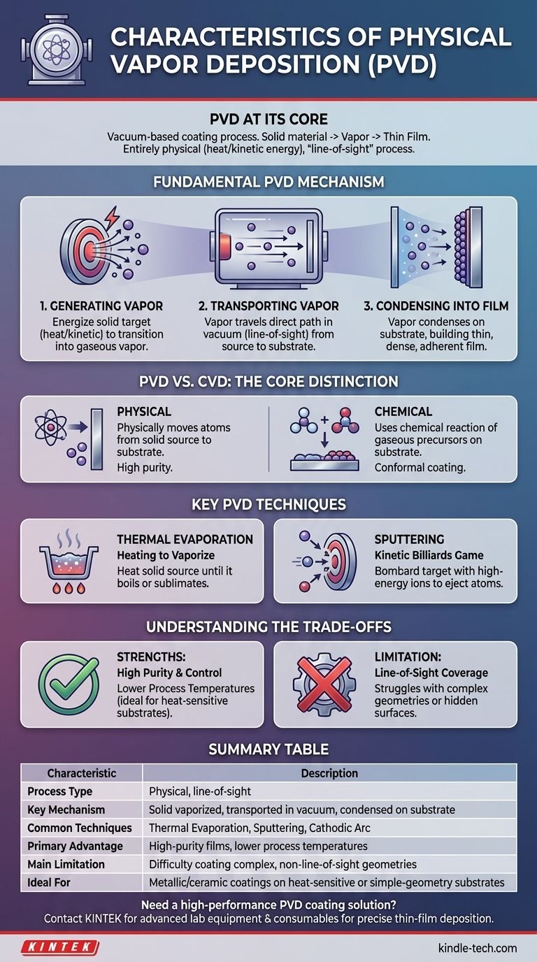
At its core, Physical Vapor Deposition (PVD) is a family of vacuum-based coating processes where a solid material is physically converted into a vapor, transported across a vacuum chamber, and condensed onto a substrate to form a high-performance thin film. Unlike chemical processes, PVD relies entirely on physical mechanisms like heat or kinetic energy to move atoms from a source to a target.
The defining characteristic of PVD is that it is a physical, "line-of-sight" process. It physically relocates atoms from a solid source to a substrate's surface without inducing a chemical reaction to create the final material.
The Fundamental PVD Mechanism: From Solid to Vapor to Film
Every PVD process follows the same fundamental three-step sequence within a high-vacuum environment. The vacuum is critical as it prevents the vaporized material from reacting with or scattering off of ambient air particles.
Step 1: Generating the Vapor
The first step is to energize a solid source material, known as the "target," until it transitions into a gaseous vapor phase. This is accomplished purely through the application of physical energy.
Step 2: Transporting the Vapor
Once vaporized, the atoms or molecules travel in a straight line through the vacuum chamber from the source to the substrate. This direct path is why PVD is often described as a line-of-sight process.
Step 3: Condensing into a Film
When the vapor particles reach the cooler surface of the substrate, they condense back into a solid state. This condensation builds up layer by layer, forming a thin, dense, and highly adherent film.
Key PVD Techniques and Their Principles
The primary difference between PVD methods lies in how they accomplish Step 1—generating the vapor. The two most common techniques illustrate this distinction perfectly.
Thermal Evaporation: Heating to Vaporize
This is the most straightforward method. A solid source material is heated in a crucible until it reaches a high enough temperature to boil or sublimate, releasing a vapor that then coats the substrate.
Sputtering: A Kinetic Billiards Game
Sputtering does not rely on heat. Instead, the target material is bombarded with high-energy ions (typically from an inert gas like argon). These ions act like microscopic cue balls, striking the target and knocking atoms loose from its surface, which then deposit onto the substrate.
Other Notable Methods
The PVD family is diverse and includes specialized techniques like Cathodic Arc Deposition (Arc-PVD), which uses an electric arc to vaporize the source, and Pulsed Laser Deposition, which uses a high-power laser to ablate material from the target.
Differentiating PVD from Chemical Vapor Deposition (CVD)
Understanding PVD is often easiest when comparing it to its counterpart, Chemical Vapor Deposition (CVD). Their names hint at their fundamental difference.
The Core Distinction: Physical vs. Chemical
PVD physically moves atoms from a solid source onto the substrate. The material on the substrate is the same as the material from the source.
CVD uses a chemical reaction on the substrate's surface to create the film. One or more precursor gases are introduced into a chamber, where they react or decompose on a hot surface to form a new, stable solid material.
Process Inputs
PVD starts with a solid target of the desired coating material. CVD starts with gaseous precursor molecules that contain the elements needed for the final film.
Understanding the Trade-offs
Like any technology, PVD has distinct advantages and inherent limitations that define its ideal applications.
Strength: Purity and Control
Because PVD operates in a high vacuum and physically transports the source material, it can produce films of exceptionally high purity. The process offers precise control over film thickness and structure.
Strength: Lower Process Temperatures
Many PVD processes, particularly sputtering, can be conducted at relatively low temperatures. This makes them ideal for coating heat-sensitive substrates, such as plastics or certain electronic components, that would be damaged by high-temperature CVD processes.
Limitation: Line-of-Sight Coverage
The "line-of-sight" nature of PVD is its most significant limitation. It excels at coating flat or gently curved surfaces but struggles to deposit a uniform film inside complex geometries, deep trenches, or on the backside of an object.
Making the Right Choice for Your Goal
Selecting between PVD and a chemical process like CVD depends entirely on the material you are depositing and the geometry of the part you are coating.
- If your primary focus is a high-purity metallic or ceramic coating on a simple geometry: PVD is often the superior choice due to its direct material transfer and lower temperature requirements.
- If your primary focus is creating a perfectly uniform (conformal) coating over a complex shape with hidden surfaces: CVD is generally the better approach, as the precursor gases can flow and react on all exposed surfaces.
Understanding this fundamental distinction between a physical transfer and a chemical creation is the key to leveraging the power of thin-film deposition technologies.
Summary Table:
| Characteristic | Description |
|---|---|
| Process Type | Physical, line-of-sight |
| Key Mechanism | Solid material vaporized, transported in vacuum, condensed on substrate |
| Common Techniques | Thermal Evaporation, Sputtering, Cathodic Arc |
| Primary Advantage | High-purity films, lower process temperatures |
| Main Limitation | Difficulty coating complex, non-line-of-sight geometries |
| Ideal For | Metallic/ceramic coatings on heat-sensitive or simple-geometry substrates |
Need a high-performance PVD coating solution for your lab or production line? KINTEK specializes in providing advanced lab equipment and consumables for precise thin-film deposition. Our expertise ensures you get the right PVD technology to achieve superior coating purity, adhesion, and performance for your specific substrates. Contact our experts today to discuss your application and discover how KINTEK can enhance your research or manufacturing process.
Visual Guide
Related Products
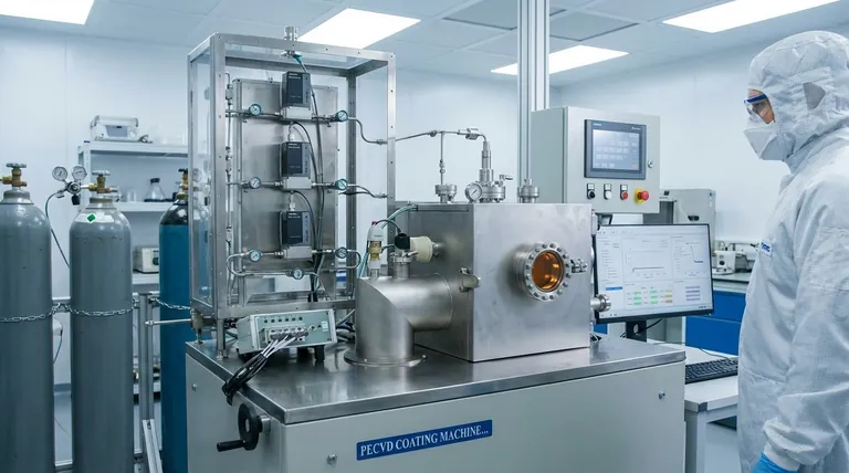
- Chemical Vapor Deposition CVD Equipment System Chamber Slide PECVD Tube Furnace with Liquid Gasifier PECVD Machine
- RF PECVD System Radio Frequency Plasma-Enhanced Chemical Vapor Deposition RF PECVD
- 915MHz MPCVD Diamond Machine Microwave Plasma Chemical Vapor Deposition System Reactor
- HFCVD Machine System Equipment for Drawing Die Nano-Diamond Coating
- Customer Made Versatile CVD Tube Furnace Chemical Vapor Deposition Chamber System Equipment
People Also Ask
- What happens during deposition chemistry? Building Thin Films from Gaseous Precursors
- How expensive is chemical vapor deposition? Understanding the True Cost of High-Performance Coating
- What is the chemical vapor deposition growth process? Build Superior Thin Films from the Atom Up
- Why is Chemical Vapor Deposition (CVD) equipment uniquely suited for constructing hierarchical superhydrophobic structures?
- What types of substrates are used in CVD to facilitate graphene films? Optimize Graphene Growth with the Right Catalyst


