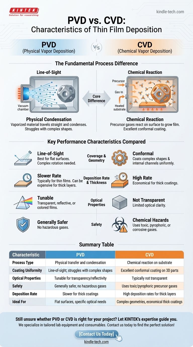
At their core, PVD and CVD are fundamentally different processes for applying thin films. Physical Vapor Deposition (PVD) is a line-of-sight process that physically transfers a material from a source to a substrate, where it condenses as a coating. In contrast, Chemical Vapor Deposition (CVD) uses precursor gases that undergo a chemical reaction directly on the substrate's surface to grow the film from the ground up.
The choice between PVD and CVD is not about which is inherently "better," but which process aligns with your specific application's requirements. PVD offers precision and material purity, while CVD excels at uniformly coating complex geometries and is often more economical for thick layers.
The Fundamental Process Difference
To choose correctly, you must first understand how each method works at a granular level. The names themselves—Physical Vapor Deposition and Chemical Vapor Deposition—reveal the primary distinction.
How PVD Works: Physical Condensation
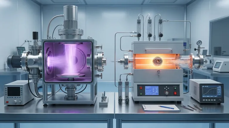
PVD is a "line-of-sight" process. A solid source material is vaporized within a vacuum chamber through methods like sputtering or evaporation.
These vaporized atoms and molecules travel in a straight line and physically condense on the substrate, forming the thin film. Think of it like spray painting, where the paint only lands on surfaces it can directly see.
How CVD Works: Chemical Reaction
CVD is a chemical process. One or more volatile precursor gases are introduced into a reaction chamber containing the substrate.
When these gases come into contact with the heated substrate, they react and decompose, leaving behind a solid material that forms the coating. This allows the film to "grow" on all exposed surfaces, even in deep recesses or holes.
Key Performance Characteristics Compared
The differences in process lead to distinct advantages and disadvantages that directly impact performance, cost, and application suitability.
Coverage and Geometry
CVD's primary advantage is its ability to create highly conformal coatings. Because the chemical reaction occurs anywhere the gas can reach, it can uniformly coat complex shapes, internal channels, and intricate 3D parts.
PVD, being a line-of-sight process, struggles with complex geometries. It excels at coating flat surfaces but requires complex part rotation and manipulation to achieve coverage on non-planar objects.
Deposition Rate and Thickness
CVD processes often have high deposition rates, making them more economical for producing the thick coatings required for certain wear or corrosion resistance applications.
PVD is typically used for thinner films, although thick coatings are possible. The process can be slower and thus more expensive for building significant thickness.
Optical Properties
PVD offers significant versatility for optical applications. The process can be finely tuned to deposit films that are transparent, reflective, or have specific colors.
CVD coatings, as a result of their growth process and chemistry, are typically not transparent. This limits their use in applications where optical clarity is a requirement.
Understanding the Trade-offs
Neither technology is a universal solution. Acknowledging their inherent limitations is critical for making an informed decision.
The Safety Factor: CVD's Chemical Hazards
A major consideration for CVD is its reliance on precursor gases that can be toxic, pyrophoric (ignite in air), or corrosive. This introduces significant safety, storage, and handling protocols that are not a major concern for most PVD processes.
The Constraint of PVD: Vacuum and Line-of-Sight
The primary drawback of PVD is its line-of-sight nature, which makes uniformly coating complex parts a significant engineering challenge. Furthermore, many PVD processes require an ultra-high vacuum, which adds to equipment complexity and cost.
The Economic Equation
CVD can be more economical for high-volume production of thick coatings on complex parts due to higher deposition rates and no need for an ultra-high vacuum. However, the costs associated with hazardous gas handling can offset these savings.
Making the Right Choice for Your Application
Your decision should be guided by your project's most critical requirement. Assess your primary goal to find the most effective and efficient path forward.
- If your primary focus is coating complex 3D shapes uniformly: CVD is the superior choice due to its non-line-of-sight deposition.
- If your primary focus is achieving specific optical properties like transparency: PVD provides the necessary control and material options.
- If your primary focus is safety and simplified material handling: PVD avoids the toxic and corrosive precursor gases associated with CVD.
- If your primary focus is producing very thick coatings economically: CVD's high deposition rates often make it the more cost-effective solution.
Understanding these core differences empowers you to select the deposition technology that directly serves your engineering goals.
Summary Table:
| Characteristic | PVD (Physical Vapor Deposition) | CVD (Chemical Vapor Deposition) |
|---|---|---|
| Process Type | Physical transfer and condensation | Chemical reaction on substrate |
| Coating Uniformity | Line-of-sight; struggles with complex shapes | Excellent conformal coating on 3D parts |
| Optical Properties | Tunable for transparency/reflectivity | Typically not transparent |
| Safety | Generally safer, no hazardous gases | Uses toxic/pyrophoric precursor gases |
| Deposition Rate | Slower for thick coatings | High deposition rates for thick layers |
| Ideal For | Flat surfaces, specific optical needs | Complex geometries, economical thick coatings |
Still unsure whether PVD or CVD is right for your project? Let KINTEK's expertise guide you. We specialize in providing tailored lab equipment and consumables for all your thin-film deposition needs. Our team can help you select the optimal technology to achieve your specific coating requirements for performance, safety, and cost-efficiency. Contact us today to discuss your application and find the perfect solution!
Visual Guide
Related Products
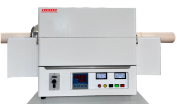
- Chemical Vapor Deposition CVD Equipment System Chamber Slide PECVD Tube Furnace with Liquid Gasifier PECVD Machine
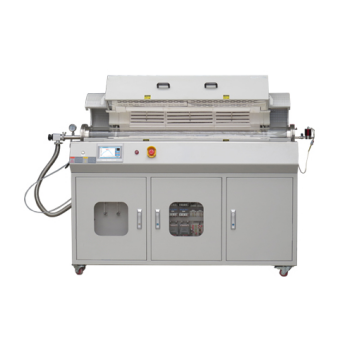
- Inclined Rotary Plasma Enhanced Chemical Vapor Deposition PECVD Equipment Tube Furnace Machine
- RF PECVD System Radio Frequency Plasma-Enhanced Chemical Vapor Deposition RF PECVD
- Customer Made Versatile CVD Tube Furnace Chemical Vapor Deposition Chamber System Equipment
- Vacuum Hot Press Furnace Machine for Lamination and Heating
People Also Ask
- What is the difference between CVD and PVD process? A Guide to Choosing the Right Coating Method
- How are PECVD and CVD different? A Guide to Choosing the Right Thin-Film Deposition Process
- What are the advantages of PECVD over CVD? Achieve High-Quality Thin Films at Lower Temperatures
- What is the difference between thermal CVD and PECVD? Choose the Right Thin-Film Deposition Method
- How is PECVD different from CVD? Unlock Low-Temperature Thin Film Deposition