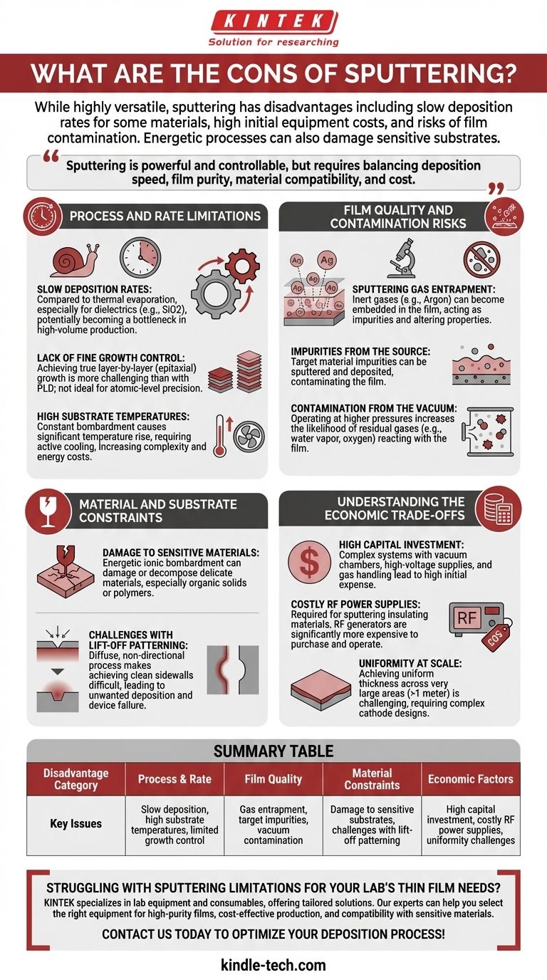
While highly versatile, the primary disadvantages of sputtering are its relatively slow deposition rates for certain materials, high initial equipment costs, and inherent risks of film contamination. The energetic nature of the process can also damage sensitive substrates or materials.
Sputtering is a powerful and controllable deposition method, but it is not without significant trade-offs. Its main drawbacks stem from the physics of ionic bombardment and the vacuum environment, creating a delicate balance between deposition speed, film purity, material compatibility, and overall cost.

Process and Rate Limitations
Sputtering is a physical process, and its mechanics impose several operational constraints that can impact manufacturing throughput and precision.
Slow Deposition Rates
Compared to thermal evaporation, sputtering can be a much slower process, especially for certain materials like dielectrics (e.g., SiO2). This can be a significant bottleneck in high-volume production environments where cycle time is critical.
Lack of Fine Growth Control
Achieving true layer-by-layer (epitaxial) growth is more challenging with sputtering than with techniques like Pulsed Laser Deposition (PLD). While sputtering offers good thickness control, it is not the ideal method for applications requiring atomic-level precision.
High Substrate Temperatures
The constant bombardment of particles can cause the substrate temperature to rise significantly. This requires active cooling systems, which add complexity, increase energy costs, and can decrease overall production rates.
Film Quality and Contamination Risks
The quality of a sputtered film is highly dependent on the process environment, which introduces several potential sources of contamination.
Sputtering Gas Entrapment
The inert gases used to create the plasma (typically Argon) can become embedded or entrapped within the growing thin film. These trapped gas atoms act as impurities and can alter the film's mechanical or electrical properties.
Impurities from the Source
The source material, or target, is never perfectly pure. Impurities within the target can be sputtered along with the desired material and deposited onto the substrate, contaminating the final film.
Contamination from the Vacuum
Sputtering often operates at a higher pressure (a poorer vacuum) than processes like evaporation. This increases the likelihood that residual gases in the chamber (like water vapor or oxygen) will react with or be incorporated into the film.
Material and Substrate Constraints
The high-energy nature of sputtering makes it unsuitable for certain types of materials and fabrication processes.
Damage to Sensitive Materials
The energetic ionic bombardment can easily damage or decompose delicate materials. This is particularly true for organic solids or polymers, which may not withstand the sputtering process.
Challenges with Lift-Off Patterning
"Lift-off" is a common technique for patterning thin films. However, sputtering is a diffuse, non-directional process, which makes achieving the clean, sharp sidewalls required for successful lift-off very difficult. This can lead to unwanted film deposition on the sidewalls of the pattern, causing device failure.
Understanding the Economic Trade-offs
Beyond the technical limitations, sputtering involves significant financial and operational considerations.
High Capital Investment
Sputtering systems are complex machines that require sophisticated vacuum chambers, high-voltage power supplies, and gas handling systems. This results in a high initial capital expense compared to simpler deposition methods.
Costly RF Power Supplies
To sputter electrically insulating materials, a Radio Frequency (RF) power supply is required instead of a simpler DC source. RF generators are significantly more expensive to purchase and operate.
Uniformity at Scale
While excellent for smaller substrates, achieving highly uniform film thickness across very large areas (e.g., >1 meter) can be challenging. It often requires complex cathode designs to ensure the plasma density is even across the entire target surface.
Is Sputtering the Right Choice for Your Application?
Choosing a deposition technique requires aligning the process capabilities with your primary goal.
- If your primary focus is high-purity films for sensitive electronics: You must account for potential gas entrapment and invest in high-purity targets and excellent vacuum systems to mitigate contamination.
- If your primary focus is high-volume manufacturing: The slow deposition rates for some materials and high energy costs must be carefully modeled to determine if the cost-per-part is acceptable.
- If your primary focus is depositing on sensitive or organic substrates: The inherent ionic bombardment and heating may make sputtering unsuitable, and alternative, "gentler" methods should be considered.
By weighing these limitations against sputtering's strengths in film adhesion and material versatility, you can make a technically sound and economically viable decision for your project.
Summary Table:
| Disadvantage Category | Key Issues |
|---|---|
| Process & Rate | Slow deposition, high substrate temperatures, limited growth control |
| Film Quality | Gas entrapment, target impurities, vacuum contamination |
| Material Constraints | Damage to sensitive substrates, challenges with lift-off patterning |
| Economic Factors | High capital investment, costly RF power supplies, uniformity challenges |
Struggling with sputtering limitations for your lab's thin film needs? KINTEK specializes in lab equipment and consumables, offering tailored solutions to overcome deposition challenges. Our experts can help you select the right equipment to ensure high-purity films, cost-effective production, and compatibility with sensitive materials. Contact us today to optimize your deposition process and achieve superior results!
Visual Guide
Related Products
- Spark Plasma Sintering Furnace SPS Furnace
- Vacuum Induction Melting Spinning System Arc Melting Furnace
- Chemical Vapor Deposition CVD Equipment System Chamber Slide PECVD Tube Furnace with Liquid Gasifier PECVD Machine
- Customer Made Versatile CVD Tube Furnace Chemical Vapor Deposition Chamber System Equipment
- Vacuum Cold Mounting Machine for Sample Preparation
People Also Ask
- What is SPS sintering method? A Guide to High-Speed, High-Performance Material Fabrication
- What technical advantages does a Spark Plasma Sintering (SPS) furnace offer for LZP ceramics? Enhance Ionic Conductivity
- What are the fundamentals of spark plasma sintering process? Unlock Rapid, High-Performance Material Consolidation
- What is the mechanism of SPS process? A Deep Dive into Rapid, Low-Temperature Sintering
- What is the theory of spark plasma sintering? A Guide to Rapid, Low-Temperature Densification


