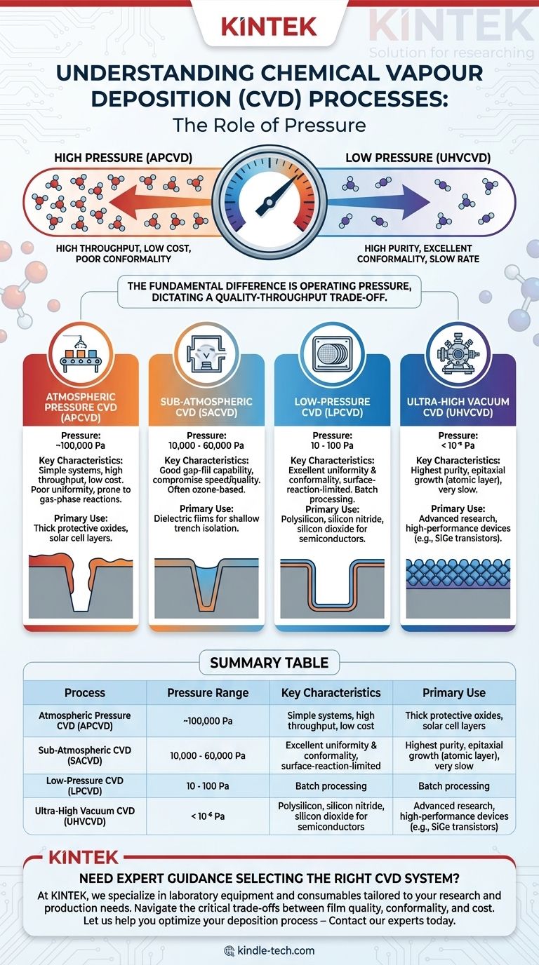
The fundamental difference between Chemical Vapor Deposition (CVD) processes is the operating pressure inside the reaction chamber. This single parameter dictates nearly everything else, from the quality and uniformity of the deposited film to the speed of the process and the cost of the equipment. While all CVD methods involve introducing reactive gases that form a solid film on a heated substrate, adjusting the pressure dramatically changes the physics of the deposition.
The core principle to understand is the trade-off between pressure and quality. Lowering the process pressure generally yields higher-purity, more uniform films that can conform to complex shapes, but it does so at the cost of slower deposition rates and more expensive, complex equipment.

The Role of Pressure in CVD
The choice between Atmospheric Pressure CVD (APCVD), Low-Pressure CVD (LPCVD), and other variants is an engineering decision rooted in the physical behavior of gases. The pressure determines how gas molecules interact with each other and with the substrate surface.
Gas Transport and Mean Free Path
At atmospheric pressure, gas molecules are densely packed and collide with each other constantly. This short "mean free path" (the average distance a molecule travels before a collision) results in a diffusion-limited process where reactants reach the substrate in a somewhat random, non-uniform way.
By lowering the pressure, the mean free path increases significantly. Molecules travel farther in straight lines, allowing them to reach all surfaces of the substrate—including the bottom and sidewalls of tiny trenches—before reacting.
Surface Reaction vs. Gas-Phase Reaction
High pressure promotes undesirable chemical reactions in the gas phase above the substrate. These reactions can form tiny particles that then fall onto the surface, creating defects and degrading film quality.
In low-pressure environments, the process becomes surface-reaction-limited. Deposition primarily occurs when the reactant gases adsorb directly onto the heated substrate, which is the desired mechanism for creating a high-quality, dense, and well-adhered film.
Conformality and Step Coverage
Conformality describes how uniformly a film coats a non-flat surface. For microelectronics with complex 3D structures, this is critical.
Because low pressure allows gas molecules to reach all surfaces before reacting, LPCVD and UHVCVD processes provide excellent conformality. High-pressure APCVD, being diffusion-limited, provides very poor conformality, creating thicker films on top surfaces and much thinner films inside trenches.
A Breakdown of Key CVD Processes
Each CVD process occupies a specific niche defined by the balance of speed, cost, and film quality.
Atmospheric Pressure CVD (APCVD)
- Pressure: Standard atmospheric pressure (~100,000 Pa).
- Characteristics: Simple, open-ended or conveyor-based systems make for very high throughput and low equipment cost.
- Film Quality: Generally low, with poor uniformity and conformality. Prone to particle contamination from gas-phase reactions.
- Primary Use: Applications where speed and cost are paramount and film perfection is not, such as depositing thick protective oxide layers or some layers in solar cell manufacturing.
Low-Pressure CVD (LPCVD)
- Pressure: Typically 10 to 100 Pa.
- Characteristics: Requires vacuum pumps and sealed chambers, increasing cost and complexity. Processes are typically run in batches of wafers.
- Film Quality: Excellent uniformity and high conformality. The deposition is driven by surface reaction, leading to high-purity films.
- Primary Use: The workhorse of the semiconductor industry for depositing high-quality polysilicon, silicon nitride, and silicon dioxide films.
Sub-Atmospheric CVD (SACVD)
- Pressure: Below atmospheric but higher than LPCVD (e.g., 10,000 to 60,000 Pa).
- Characteristics: A compromise designed to achieve better film properties than APCVD but with higher deposition rates than LPCVD.
- Film Quality: Good, especially for filling high-aspect-ratio gaps (a process known as gap-fill). It often uses ozone-based chemistry.
- Primary Use: Depositing dielectric films like silicon dioxide for shallow trench isolation in integrated circuits.
Ultra-High Vacuum CVD (UHVCVD)
- Pressure: Extremely low, below 10⁻⁶ Pa.
- Characteristics: Requires very expensive and complex vacuum systems. Deposition rates are extremely slow.
- Film Quality: The highest possible purity and control. It can deposit films one atomic layer at a time (epitaxy), creating perfect crystal structures.
- Primary Use: Advanced research and fabrication of high-performance devices, such as growing strained silicon-germanium (SiGe) epitaxial layers for high-speed transistors.
Understanding the Core Trade-offs
Choosing a CVD process is never about finding the "best" one, but the most appropriate one. The decision always involves navigating a set of fundamental trade-offs.
Quality vs. Throughput
This is the most critical trade-off. APCVD offers unmatched throughput but produces low-quality films. UHVCVD produces atomically perfect films but is far too slow for mass production. LPCVD sits at a valuable sweet spot for many microelectronics applications.
Conformality vs. Cost
If your device has deep trenches or complex 3D features, you need the high conformality provided by a low-pressure process. This capability, however, comes at the direct cost of more expensive vacuum equipment, maintenance, and longer processing times.
Purity vs. Rate
The extremely clean environment of UHVCVD is necessary for creating epitaxial films free from contaminants. This cleanliness is achieved by minimizing background gases, which also means slowing down the introduction of reactant gases, thus drastically reducing the deposition rate.
Selecting the Right CVD Process
Your choice must be driven by the specific requirements of the film you need to create.
- If your primary focus is high throughput and low cost: APCVD is the most suitable choice, especially for thick, non-critical films.
- If your primary focus is high-quality, uniform films for microelectronics: LPCVD provides the best balance of quality, conformality, and acceptable production rates.
- If your primary focus is creating ultra-pure, single-crystal layers for advanced devices: UHVCVD is the only option, despite its high cost and slow speed.
- If your primary focus is filling challenging topographical gaps quickly: SACVD offers a valuable compromise between the speed of higher-pressure systems and the quality of LPCVD.
Choosing the correct CVD method is a critical engineering decision that balances the desired film characteristics against the practical constraints of production speed and cost.
Summary Table:
| Process | Pressure Range | Key Characteristics | Primary Use |
|---|---|---|---|
| APCVD | ~100,000 Pa | High throughput, low cost, simple system | Thick protective oxides, some solar cell layers |
| LPCVD | 10 - 100 Pa | Excellent uniformity & conformality, batch processing | Polysilicon, silicon nitride, silicon dioxide for semiconductors |
| SACVD | 10,000 - 60,000 Pa | Good gap-fill capability, compromise between APCVD & LPCVD | Dielectric films for shallow trench isolation |
| UHVCVD | < 10⁻⁶ Pa | Highest purity, epitaxial growth, very slow deposition | Advanced research, high-performance devices like SiGe transistors |
Need expert guidance selecting the right CVD system for your specific application?
At KINTEK, we specialize in providing laboratory equipment and consumables tailored to your research and production needs. Whether you require high-throughput APCVD for cost-effective coatings or ultra-pure UHVCVD for advanced semiconductor work, our team can help you navigate the critical trade-offs between film quality, conformality, and cost.
Let us help you optimize your deposition process – Contact our experts today to discuss your requirements and find the perfect CVD solution for your lab!
Visual Guide
Related Products
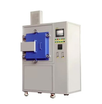
- Customer Made Versatile CVD Tube Furnace Chemical Vapor Deposition Chamber System Equipment
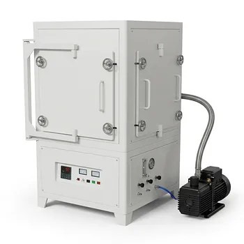
- Multi Heating Zones CVD Tube Furnace Machine Chemical Vapor Deposition Chamber System Equipment
- Horizontal High Temperature Graphite Vacuum Graphitization Furnace
- Vertical High Temperature Graphite Vacuum Graphitization Furnace
- Controlled Nitrogen Inert Hydrogen Atmosphere Furnace
People Also Ask
- What is a CVD tube furnace? A Complete Guide to Thin-Film Deposition
- What is the substrate for CVD process? Choosing the Right Foundation for Your Thin Film
- What is the temperature of a CVD furnace? From 200°C to 1600°C for Precise Film Deposition
- What is the meaning of synthesis of graphene? A Guide to Top-Down vs. Bottom-Up Methods
- How is graphene synthesized? Choosing the Right Method for Your Application