In MEMS fabrication, Chemical Vapor Deposition (CVD) is not a single process but a family of techniques, each distinguished by its operating pressure and energy source. The most common types are Low-Pressure CVD (LPCVD), Plasma-Enhanced CVD (PECVD), and Atmospheric Pressure CVD (APCVD). Each method is chosen based on the specific requirements for film quality, deposition temperature, and the complexity of the device structure.
The crucial insight is that the choice between different CVD methods is a fundamental engineering trade-off. You are primarily balancing deposition temperature against film quality and the ability to uniformly coat complex shapes—a property known as conformality.

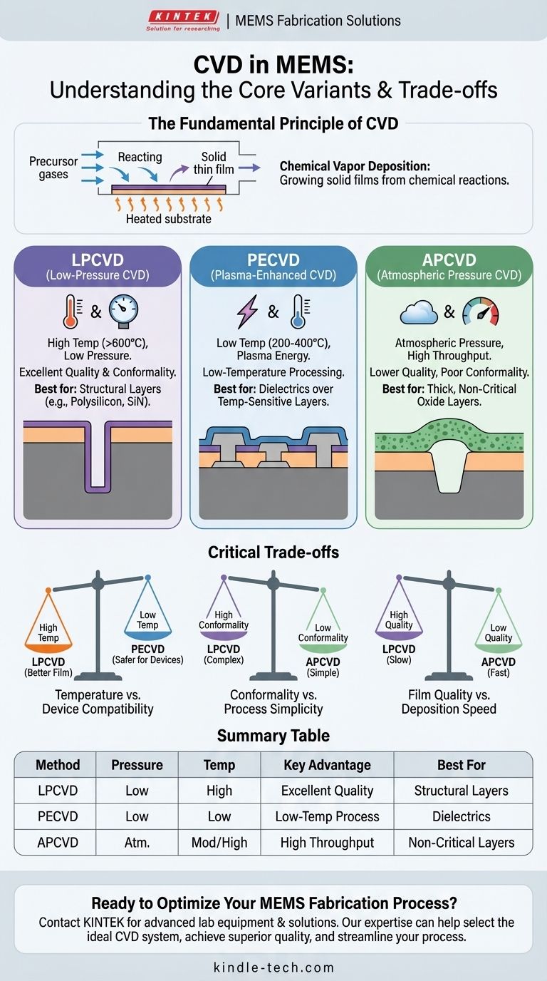
The Fundamental Principle of CVD
What is Chemical Vapor Deposition?
Chemical Vapor Deposition is a process where a solid thin film is grown on a substrate through a chemical reaction. Volatile precursor gases are introduced into a reaction chamber where they decompose or react on the heated substrate surface.
This chemical reaction distinguishes CVD from Physical Vapor Deposition (PVD), which is a purely physical process like evaporation or sputtering. In CVD, the deposited material is the product of a controlled chemical transformation.
Why CVD is Critical for MEMS
CVD is indispensable in MEMS for building the microscopic structures that define the device. It is used to deposit a wide range of materials that serve as structural layers (like polysilicon), insulating dielectrics (like silicon nitride and silicon dioxide), and protective passivation layers.
The ability to control the material properties and microstructure—whether amorphous, polycrystalline, or monocrystalline—makes CVD a uniquely versatile tool for device fabrication.
The Core CVD Variants in MEMS Fabrication
LPCVD: The High-Quality Standard
Low-Pressure Chemical Vapor Deposition (LPCVD) operates at very low pressures and typically high temperatures (often >600°C). The low pressure reduces unwanted gas-phase reactions and increases the mean free path of gas molecules.
This results in films with excellent purity, uniformity, and outstanding conformality. Conformality is the ability to coat stepped or uneven surfaces uniformly, which is critical for complex, 3D MEMS structures. LPCVD is the go-to method for depositing high-quality polysilicon and silicon nitride films.
PECVD: The Low-Temperature Workhorse
Plasma-Enhanced Chemical Vapor Deposition (PECVD) uses an energy-rich plasma to dissociate the precursor gases. This plasma provides the energy for the chemical reaction, rather than relying solely on high temperatures.
The key advantage of PECVD is its significantly lower deposition temperature (typically 200-400°C). This makes it ideal for depositing films later in the fabrication process, after temperature-sensitive components like aluminum metallization have already been created.
APCVD: The High-Throughput Option
Atmospheric Pressure Chemical Vapor Deposition (APCVD) is the simplest variant, operating at normal atmospheric pressure. Its lack of a vacuum system allows for high throughput and lower equipment costs.
However, the high pressure leads to more gas-phase reactions, resulting in lower film quality and poor conformality. Its use in modern MEMS is often limited to depositing thick, non-critical dielectric layers, such as silicon dioxide, where speed is more important than precision.
Understanding the Critical Trade-offs
Temperature vs. Device Compatibility
The most significant trade-off is process temperature. The high temperatures of LPCVD produce superior films but can damage or alter previously fabricated layers on a wafer.
If you are depositing a final passivation layer on a fully formed MEMS device with metal contacts, the high heat of LPCVD would destroy it. In this scenario, the low temperature of PECVD is the only viable option.
Conformality vs. Process Simplicity
Conformality is a measure of how well a film covers the topography of a substrate. For MEMS devices with deep trenches or complex moving parts, high conformality is non-negotiable.
LPCVD excels here, providing a nearly perfect coating over any surface. In contrast, APCVD and, to a lesser extent, PECVD, produce "line-of-sight" deposition that results in poor coverage in trenches and corners.
Film Quality vs. Deposition Speed
LPCVD films are dense, pure, and have low residual stress, making them ideal for structural components. However, the process is relatively slow.
APCVD is very fast but produces porous, lower-density films. PECVD sits in the middle, offering reasonable quality at lower temperatures, but the incorporated hydrogen and other by-products can affect film properties.
Making the Right Choice for Your Application
The best CVD method depends entirely on the specific requirements of your fabrication step and device.
- If your primary focus is creating high-purity, uniform structural layers: Use LPCVD for its superior film quality and excellent conformality, especially for polysilicon and silicon nitride.
- If your primary focus is depositing a dielectric or passivation film on a temperature-sensitive substrate: Use PECVD to avoid damaging underlying metallic or previously fabricated components.
- If your primary focus is the rapid, low-cost deposition of a thick, non-critical oxide layer: Consider APCVD for its high throughput, accepting the trade-off of lower quality and poor conformality.
By understanding these core trade-offs, you can strategically select the CVD process that ensures the performance and reliability of your MEMS device.
Summary Table:
| CVD Method | Operating Pressure | Typical Temperature | Key Advantage | Best For |
|---|---|---|---|---|
| LPCVD | Low Pressure (< 1 Torr) | High (> 600°C) | Excellent film quality & conformality | High-purity structural layers (polysilicon, silicon nitride) |
| PECVD | Low Pressure | Low (200-400°C) | Low-temperature processing | Dielectrics on temperature-sensitive substrates |
| APCVD | Atmospheric Pressure | Moderate to High | High throughput & low cost | Thick, non-critical oxide layers |
Ready to Optimize Your MEMS Fabrication Process?
Choosing the right CVD method is critical for your device's performance and yield. At KINTEK, we specialize in providing advanced lab equipment and consumables for MEMS research and production. Our expertise can help you:
- Select the ideal CVD system for your specific application
- Achieve superior film quality and device reliability
- Streamline your fabrication process for better results
Let's discuss how our solutions can enhance your MEMS development. Contact our experts today for a personalized consultation!
Visual Guide
Related Products
- Chemical Vapor Deposition CVD Equipment System Chamber Slide PECVD Tube Furnace with Liquid Gasifier PECVD Machine
- Customer Made Versatile CVD Tube Furnace Chemical Vapor Deposition Chamber System Equipment
- HFCVD Machine System Equipment for Drawing Die Nano-Diamond Coating
- Multi Heating Zones CVD Tube Furnace Machine Chemical Vapor Deposition Chamber System Equipment
- CVD Diamond Dressing Tools for Precision Applications
People Also Ask
- What types of substrates are used in CVD to facilitate graphene films? Optimize Graphene Growth with the Right Catalyst
- Why is Chemical Vapor Deposition (CVD) equipment uniquely suited for constructing hierarchical superhydrophobic structures?
- What are the processes of vapor phase deposition? Understand CVD vs. PVD for Superior Thin Films
- What are the core advantages of PE-CVD in OLED encapsulation? Protect Sensitive Layers with Low-Temp Film Deposition
- How are carbon nanotubes grown? Master Scalable Production with Chemical Vapor Deposition


