While a powerful and widely used technique, DC magnetron sputtering has several key disadvantages that are critical to understand before selecting it for a project. The primary limitations involve its inability to deposit insulating materials, inherent process inefficiencies like poor target utilization, significant substrate heating, and the high initial cost and complexity of the equipment.
The core limitations of DC magnetron sputtering stem from its reliance on a direct current. This fundamentally restricts it to conductive materials and introduces operational inefficiencies and thermal challenges that must be carefully managed.
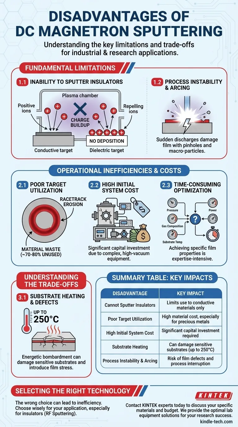
Fundamental Material and Process Limitations
The most significant drawbacks of DC magnetron sputtering are rooted in the physics of how it operates. These limitations can be a complete barrier for certain applications.
Inability to Sputter Insulators
The single greatest disadvantage is that DC magnetron sputtering cannot deposit insulating (dielectric) materials. A DC voltage requires a continuous conductive path to function.
When sputtering an insulating target, positive ions from the plasma that strike the target surface cannot be neutralized. This leads to a rapid buildup of positive charge on the target's surface, which effectively repels incoming ions and extinguishes the plasma, stopping the deposition process entirely.
Process Instability and Arcing
Even with conductive targets, process instabilities can occur. The plasma's behavior can be sensitive to pressure, power, and target condition.
This can sometimes lead to arcing, where a sudden discharge occurs on the target surface. Arcing can damage the thin film by creating macro-particles or pinholes, compromising the quality of the final coating.
Operational Inefficiencies and Costs
Beyond its material limitations, DC magnetron sputtering presents several practical challenges related to cost and efficiency that impact its viability for industrial production.
Poor Target Material Utilization
The magnetic field used to confine the plasma creates a concentrated erosion zone on the target, commonly known as the "racetrack."
This means that material is only sputtered from this specific ring, leaving a significant portion of the expensive target material unused. This low utilization rate is a major cost driver, especially when sputtering precious metals like gold or platinum.
High Initial System Cost
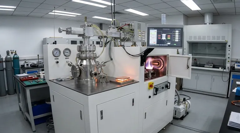
Magnetron sputtering systems are complex pieces of equipment. They require a high-vacuum chamber, multiple gas-flow controllers, a high-power DC supply, and a sophisticated magnetron cathode assembly.
This complexity results in a high initial capital investment compared to some other deposition techniques like thermal evaporation.
Time-Consuming Process Optimization
Achieving a film with specific properties (like stress, resistivity, or optical constants) can be challenging.
The final film quality is dependent on numerous control parameters, including pressure, power, gas composition, and substrate temperature. Optimizing this multi-variable process can be a time-consuming and expertise-intensive task.
Understanding the Trade-offs
It is crucial to view these disadvantages as trade-offs for the benefits the technique provides. The same physical phenomena that cause limitations are also responsible for its strengths.
Substrate Heating and Film Defects
The energetic bombardment of the substrate by sputtered atoms and plasma ions is what creates dense, strongly adhered films.
However, this same bombardment transfers significant energy, leading to substrate heating, which can reach up to 250°C. This can damage sensitive substrates and may also introduce structural defects or stress into the growing film.
Deposition Rate: A Matter of Perspective
Compared to simple diode sputtering, magnetron sputtering offers a much higher deposition rate for conductive materials, making it suitable for industrial production.
However, the statement that it has a "slow" deposition rate often comes from comparison to other techniques like evaporation, or when considering that the rate for dielectric materials is effectively zero.
Making the Right Choice for Your Application
Choosing the correct deposition method requires matching the technology's capabilities and limitations to your project goals.
- If your primary focus is depositing conductive films (metals, alloys, TCOs) with high density and adhesion: DC magnetron sputtering is an excellent choice, but you must plan for the costs of poor target utilization and manage potential substrate heating.
- If your primary focus is depositing insulating or dielectric films (like SiO₂, Al₂O₃, or nitrides): DC magnetron sputtering is the wrong tool. You must use a technique like RF (Radio Frequency) sputtering, which overcomes the charge buildup issue.
- If your primary focus is R&D with a limited budget or heat-sensitive substrates: The high equipment cost and inherent substrate heating may make other techniques, such as thermal evaporation, a more practical starting point.
Understanding these limitations is the first step to selecting the right deposition technology for your specific application.
Summary Table:
| Disadvantage | Key Impact |
|---|---|
| Cannot Sputter Insulators | Limits use to conductive materials only |
| Poor Target Utilization | High material cost, especially for precious metals |
| High Initial System Cost | Significant capital investment required |
| Substrate Heating | Can damage sensitive substrates (up to 250°C) |
| Process Instability & Arcing | Risk of film defects and process interruption |
Need help selecting the right sputtering technology for your specific materials and budget? The limitations of DC magnetron sputtering highlight the importance of choosing the correct lab equipment for your application. At KINTEK, we specialize in lab equipment and consumables, serving diverse laboratory needs. Our experts can help you navigate these trade-offs and find the optimal solution—whether it's an RF sputtering system for dielectrics or a different deposition technique altogether. Contact us today to discuss your project requirements and ensure you get the performance and value your research deserves!
Visual Guide
Related Products
- Microwave Plasma Chemical Vapor Deposition MPCVD Machine System Reactor for Lab and Diamond Growth
- Laboratory CVD Boron Doped Diamond Materials
- 915MHz MPCVD Diamond Machine Microwave Plasma Chemical Vapor Deposition System Reactor
- Molybdenum Tungsten Tantalum Special Shape Evaporation Boat
- HFCVD Machine System Equipment for Drawing Die Nano-Diamond Coating
People Also Ask
- How does a microwave plasma reactor facilitate the synthesis of diamond? Master MPCVD with Precision Technology
- What are the advantages of a Microwave Plasma CVD reactor for MCD/NCD coatings? Precision Multilayer Diamond Engineering
- How is a diamond formed from CVD? The Science of Growing Diamonds Atom by Atom
- How do vacuum pumps and valves collaborate in MPCVD? Achieve Precise Pressure Control for Superior CNT Synthesis
- What are the primary advantages of the CVD method for growing diamonds? Engineering High-Purity Gems and Components


