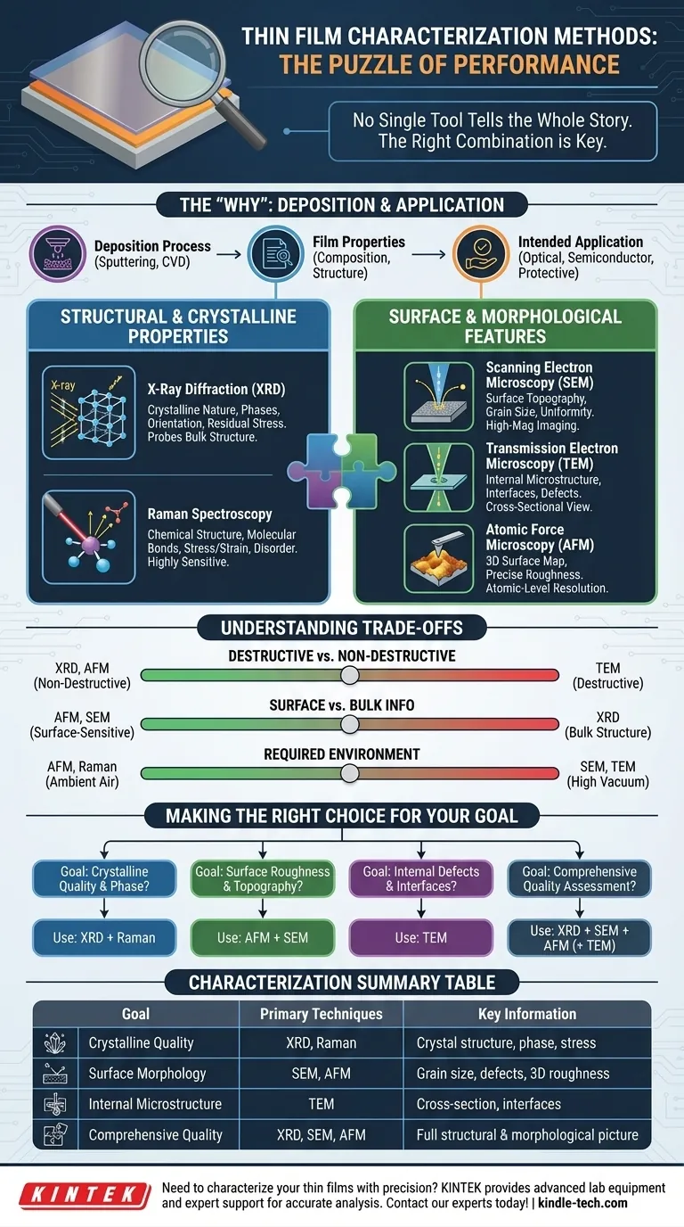
To characterize a thin film, a suite of specialized techniques is used to analyze its structural, morphological, and functional properties. The most common methods include X-ray Diffraction (XRD) and Raman Spectroscopy for understanding the film's crystalline and chemical structure, alongside various microscopy techniques like Scanning Electron Microscopy (SEM), Transmission Electron Microscopy (TEM), and Atomic Force Microscopy (AFM) for visualizing its surface and internal features.
The core challenge in thin film analysis is not finding a single, perfect tool, but rather selecting the right combination of methods. Each technique provides a different piece of the puzzle, and a comprehensive understanding requires measuring the specific properties—from atomic structure to surface roughness—that dictate the film's performance in its final application.
Understanding the "Why": Key Properties of a Film
Before choosing a characterization method, you must first define what you need to measure. The properties of a thin film are a direct result of its composition and the deposition method used to create it, such as sputtering, chemical vapor deposition (CVD), or spin coating.
Characterization is the process of verifying that the deposition process achieved the desired outcome. These outcomes are tied directly to the film's intended application, whether it's for an optical coating, a semiconductor device, or a protective layer.
Analyzing Structural and Crystalline Properties
This category of techniques probes the very foundation of the film: how its atoms are arranged. This is critical for understanding its electrical, optical, and mechanical behavior.
X-ray Diffraction (XRD)
XRD is the primary tool for determining the crystalline nature of a film. It can distinguish between an amorphous (disordered) structure and a crystalline (ordered) one.
It also identifies the specific crystal phases present, their orientation, and can be used to measure residual stress within the film.
Raman Spectroscopy
Raman Spectroscopy provides insight into the chemical structure and molecular bonds. It is highly sensitive to subtle changes in crystallography and can detect stress, strain, and disorder in the material.
This makes it invaluable for confirming material composition and quality, especially in semiconductor and carbon-based films.
Visualizing Surface and Morphological Features
Morphology refers to the film's physical form, including its surface texture, grain structure, and any defects. These features are often controlled by the deposition process and are critical for performance.
Field Emission-Scanning Electron Microscopy (FE-SEM)
SEM provides high-magnification images of the film's surface topography. It is the workhorse for visualizing features like grain size, micro-cracks, and surface uniformity.
Higher-resolution versions, like FE-SEM, allow for incredibly detailed surface inspection.
Transmission Electron Microscopy (TEM)
While SEM looks at the surface, TEM looks through a very thin slice of the film. This reveals the internal microstructure in cross-section.
TEM is essential for observing grain boundaries, crystal defects, and the interface between different layers in a multi-layered film.
Atomic Force Microscopy (AFM)
AFM creates a three-dimensional map of the film's surface with atomic-level resolution. Its primary use is for precisely quantifying surface roughness.
Unlike electron microscopes, AFM does not require a vacuum and can operate on a wide variety of materials without special preparation.
Understanding the Trade-offs
No single technique tells the whole story. Choosing the right method involves understanding the practical limitations and the type of information each one provides.
Destructive vs. Non-Destructive
Some methods, like XRD and AFM, are generally non-destructive, meaning the sample can be used for other tests or in a device afterward.
Conversely, preparing a sample for TEM requires cutting out a very thin slice, which is a destructive process.
Surface vs. Bulk Information
Techniques like AFM and SEM are highly surface-sensitive, providing information only about the top few nanometers of the film.
XRD, on the other hand, probes deeper into the material, providing information about the bulk structure of the film.
Required Sample Environment
Electron microscopes (SEM and TEM) require the sample to be in a high vacuum, which can limit the types of materials that can be studied.
Techniques like AFM and Raman Spectroscopy can be performed in ambient air, offering greater flexibility.
Making the Right Choice for Your Goal
Your primary objective dictates the characterization strategy. A combination of techniques is nearly always required for a complete picture.
- If your primary focus is crystalline quality and phase purity: Start with XRD to confirm the fundamental structure and complement with Raman Spectroscopy to check for stress and chemical bonding.
- If your primary focus is surface roughness and topography: Use AFM for precise, quantitative roughness measurements and SEM for a broader, qualitative view of the surface morphology.
- If your primary focus is internal defects and layer interfaces: TEM is the essential tool, as it is the only method that directly visualizes the film's cross-sectional microstructure.
- If your primary focus is a comprehensive quality assessment: A typical workflow involves XRD for structure, SEM for surface morphology, and AFM for surface roughness, with TEM reserved for detailed defect analysis.
Ultimately, selecting the right characterization methods is how you transform an invisible, microscopic layer into a reliable and well-understood component.
Summary Table:
| Characterization Goal | Recommended Primary Technique(s) | Key Information Provided |
|---|---|---|
| Crystalline Quality & Phase | XRD, Raman Spectroscopy | Crystal structure, phase identification, stress/strain |
| Surface Morphology & Topography | SEM, AFM | Grain size, surface features, defects, 3D roughness map |
| Internal Microstructure & Interfaces | TEM | Cross-sectional view, grain boundaries, layer interfaces |
| Comprehensive Quality Assessment | Combination of XRD, SEM, AFM | Full picture of structural and morphological properties |
Need to characterize your thin films with precision?
Choosing the right combination of characterization techniques is critical to understanding your film's performance. KINTEK specializes in providing the advanced lab equipment and expert support you need for accurate thin film analysis.
We help you:
- Select the right tools for your specific material and application goals.
- Achieve reliable results with high-performance equipment for techniques like XRD, SEM, and more.
- Optimize your workflow with solutions tailored to your laboratory's needs.
Let's discuss your thin film characterization challenges. Contact our experts today to find the perfect solution for your research or quality control.
Visual Guide