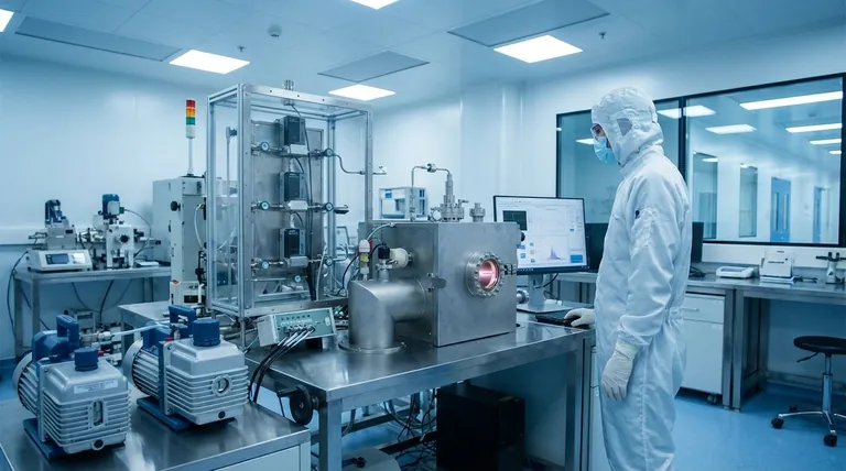
In nanotechnology, deposition methods are techniques used to apply ultra-thin films of material, often just a few atoms thick, onto a surface or substrate. The two primary categories of these methods are Physical Vapor Deposition (PVD), which includes processes like magnetron sputtering, and Chemical Vapor Deposition (CVD), where precursor gases react to form the film. These techniques are fundamental because they allow for subnanometer-level control over thickness and material properties.
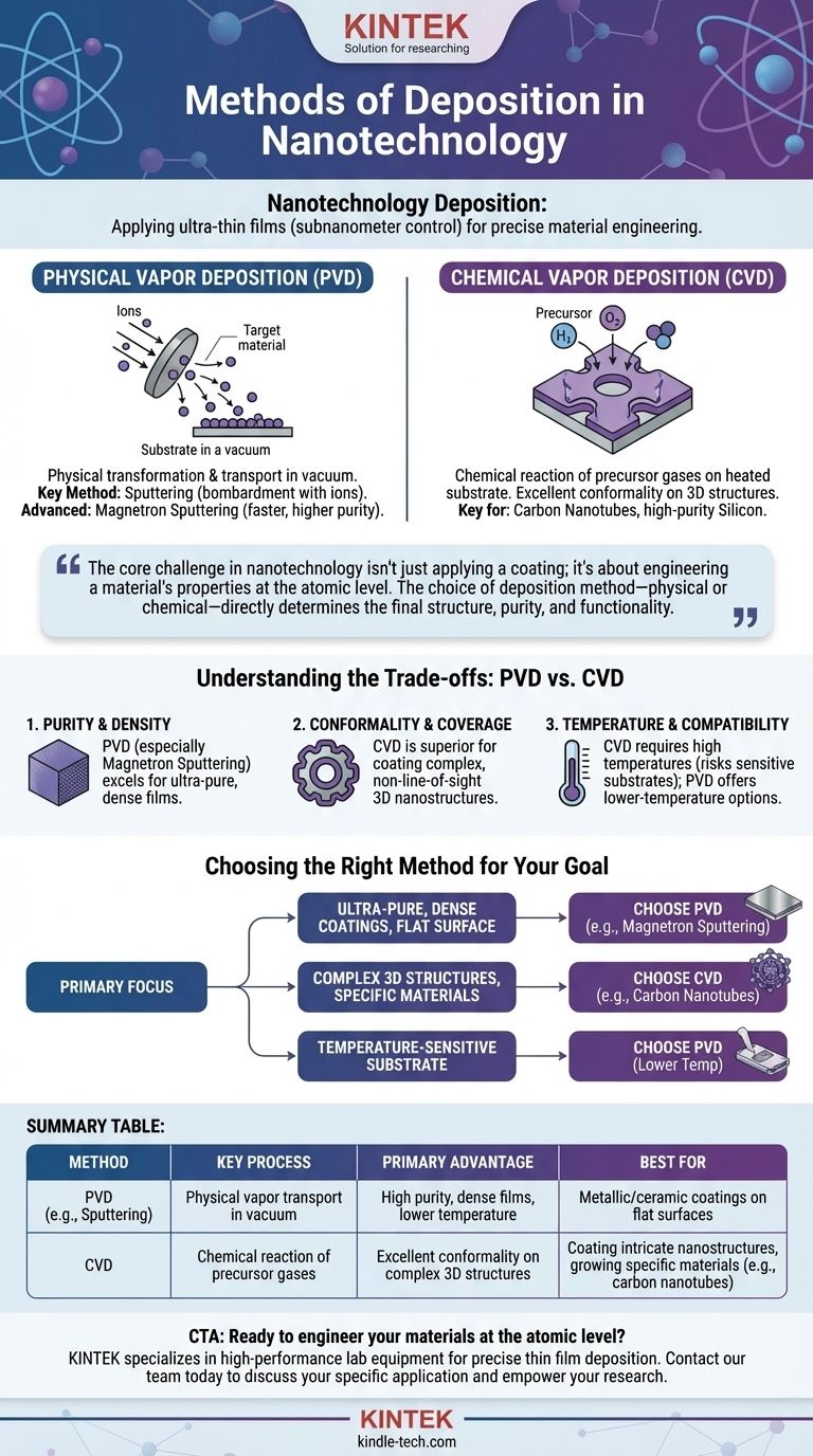
The core challenge in nanotechnology isn't just applying a coating; it's about engineering a material's properties at the atomic level. The choice of deposition method—physical or chemical—directly determines the final structure, purity, and functionality of the nanoscale device or surface being created.
The Two Pillars of Nanoscale Deposition
At the highest level, deposition techniques are separated by how they transport material from a source to the substrate. This distinction is critical because it dictates the characteristics of the resulting thin film. The two main families are Physical Vapor Deposition (PVD) and Chemical Vapor Deposition (CVD).
Physical Vapor Deposition (PVD)
PVD encompasses methods where a material is physically transformed into a vapor phase, transported through a vacuum or low-pressure environment, and then condensed onto the substrate as a thin film. This is fundamentally a mechanical or thermal process.
Key PVD Method: Sputtering
Sputtering involves bombarding a solid source material, known as a "target," with high-energy ions. This bombardment physically knocks atoms off the target, which then travel and deposit onto the substrate.
Magnetron sputtering is an advanced form of this technique that uses strong magnetic fields to trap electrons near the target, increasing the efficiency of the ion bombardment. This results in faster deposition rates and higher-purity films with fewer defects, making it a workhorse for many nanotechnology applications.
Chemical Vapor Deposition (CVD)
Unlike PVD, CVD is a chemical process. In this method, the substrate is exposed to one or more volatile precursor gases. These gases react or decompose on the substrate's surface, leaving behind the desired solid material.
The CVD Process
The substrate is typically heated to provide the energy needed to initiate the chemical reaction. The byproducts of the reaction are then removed by a gas flow. Because the film is built through a surface chemical reaction, CVD is exceptionally good at creating uniform, conformal layers that can coat complex, three-dimensional nanostructures.
Why CVD is Critical for Nanotechnology
CVD enables the growth of highly specific materials that are difficult to produce otherwise. It is a key method for creating advanced materials like carbon nanotubes and high-purity silicon layers for microelectronics, forming the backbone of many next-generation nanotechnologies.
Understanding the Trade-offs: PVD vs. CVD
Choosing the correct deposition method requires understanding the inherent compromises between different techniques. The right choice depends entirely on the material being deposited and the desired outcome.
Purity and Density
PVD methods, especially magnetron sputtering, are renowned for producing very dense films with extremely high purity. The vacuum environment minimizes the inclusion of unwanted contaminants.
Conformality and Coverage
CVD is the clear winner for coating complex topographies. Because the deposition is driven by a surface chemical reaction, it can uniformly coat intricate, non-line-of-sight structures, whereas PVD is often limited to what is directly in front of the source.
Temperature and Substrate Compatibility
CVD processes often require very high substrate temperatures to drive the chemical reactions. This can damage or destroy sensitive substrates, such as plastics or certain electronic components. Many PVD processes can be performed at much lower temperatures.
Choosing the Right Method for Your Nanotechnology Goal
The decision between PVD and CVD is not about which is "better," but which is the right tool for a specific engineering task.
- If your primary focus is creating ultra-pure, dense metallic or ceramic coatings on a relatively flat surface: PVD methods like magnetron sputtering offer superior control over purity and density.
- If your primary focus is coating complex 3D nanostructures or growing specific materials like carbon nanotubes: CVD is the ideal approach due to its excellent conformality and chemical specificity.
- If your primary focus is depositing a film on a temperature-sensitive substrate: A lower-temperature PVD process is almost always the more practical and effective solution.
Ultimately, selecting the right deposition technique is the foundational step in engineering functional materials at the nanoscale.
Summary Table:
| Method | Key Process | Primary Advantage | Best For |
|---|---|---|---|
| PVD (e.g., Sputtering) | Physical vapor transport in vacuum | High purity, dense films, lower temperature | Metallic/ceramic coatings on flat surfaces |
| CVD | Chemical reaction of precursor gases | Excellent conformality on complex 3D structures | Coating intricate nanostructures, growing specific materials (e.g., carbon nanotubes) |
Ready to engineer your materials at the atomic level? The choice between PVD and CVD is critical for your nanotechnology project's success. KINTEK specializes in providing high-performance lab equipment and consumables for precise thin film deposition. Our experts can help you select the right tools to achieve ultra-pure coatings or conformal layers on complex nanostructures. Contact our team today to discuss your specific application and discover how KINTEK can empower your nanotechnology research and development.
Visual Guide
Related Products
- Customer Made Versatile CVD Tube Furnace Chemical Vapor Deposition Chamber System Equipment
- Chemical Vapor Deposition CVD Equipment System Chamber Slide PECVD Tube Furnace with Liquid Gasifier PECVD Machine
- Custom CVD Diamond Coating for Lab Applications
- CVD Diamond for Thermal Management Applications
- RF PECVD System Radio Frequency Plasma-Enhanced Chemical Vapor Deposition RF PECVD
People Also Ask
- What is chemical vapor deposition for CNT? The Leading Method for Scalable Carbon Nanotube Synthesis
- What is the meaning of synthesis of graphene? A Guide to Top-Down vs. Bottom-Up Methods
- What is the effect of temperature on graphene oxide? Master Thermal Reduction for Precise Material Properties
- What is a CVD furnace? The Ultimate Guide to Precision Thin-Film Coating
- What method is used to grow graphene? Master High-Quality Production with CVD


