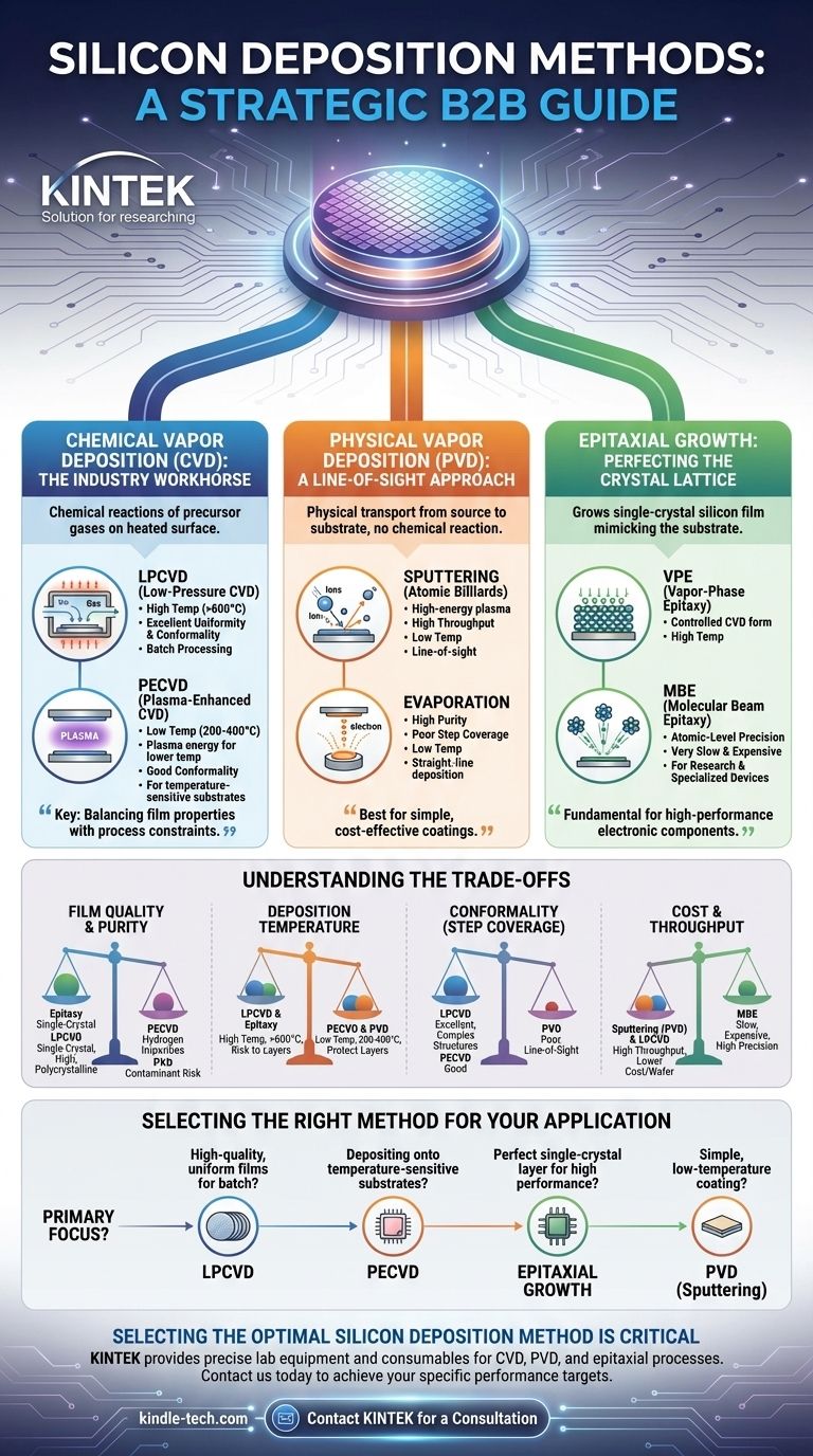
The primary methods for silicon deposition fall into three main families: Chemical Vapor Deposition (CVD), Physical Vapor Deposition (PVD), and Epitaxial Growth. CVD uses chemical reactions of precursor gases on a heated surface, PVD uses physical means like sputtering to transfer silicon to a substrate, and Epitaxy grows a single-crystal silicon layer that mimics the underlying substrate.
The choice of a silicon deposition method is not about finding the "best" technique, but about making a strategic trade-off. You must balance the required film properties—such as crystal quality, purity, and uniformity—against the process constraints of temperature, cost, and throughput.
Chemical Vapor Deposition (CVD): The Industry Workhorse
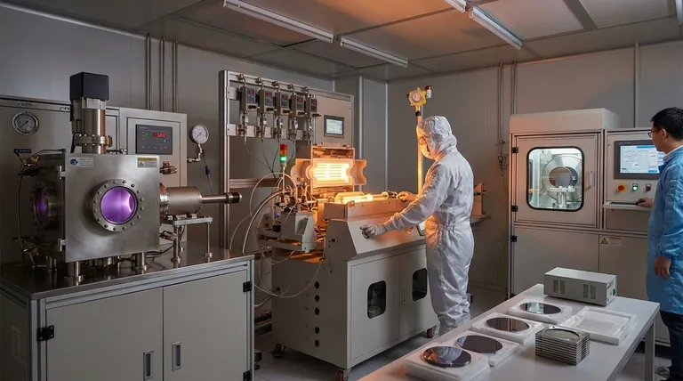
CVD is the most common method for depositing high-quality silicon films in semiconductor manufacturing. It involves flowing a silicon-containing precursor gas over a heated substrate, causing a chemical reaction that deposits a solid silicon film.
The Core Principle of CVD
A precursor gas, such as silane (SiH₄) or dichlorosilane (SiH₂Cl₂), is introduced into a reaction chamber. Thermal energy breaks down these gas molecules, allowing silicon atoms to deposit and form a film on the substrate surface.
LPCVD: For High-Quality, Conformal Films
Low-Pressure Chemical Vapor Deposition (LPCVD) is performed at high temperatures (typically >600°C) and reduced pressures.
This process is known for producing films with excellent uniformity and conformality, meaning it can evenly coat complex, three-dimensional structures. It is ideal for batch processing, allowing many wafers to be coated at once.
PECVD: The Low-Temperature Alternative
Plasma-Enhanced Chemical Vapor Deposition (PECVD) uses an electromagnetic field (plasma) to provide the energy needed to break down the precursor gases.
This critical difference allows deposition at much lower temperatures (200-400°C). PECVD is essential when depositing silicon onto substrates that cannot withstand the high heat of an LPCVD process, such as those with previously deposited metal layers.
Physical Vapor Deposition (PVD): A Line-of-Sight Approach
PVD methods physically transport silicon from a source (or "target") to the substrate without a chemical reaction. These are typically lower-temperature processes but struggle with coating complex surfaces evenly.
Sputtering: Atomic Billiards
In sputtering, a high-energy plasma of an inert gas (like Argon) is created. Ions from this plasma are accelerated to strike a solid silicon target, physically knocking silicon atoms off the surface. These ejected atoms then travel and deposit onto the substrate.
Evaporation: High Purity, Poor Coverage
Electron-beam evaporation uses a focused beam of electrons to heat a silicon source in a high-vacuum chamber until it evaporates. The resulting silicon vapor travels in a straight line and condenses on the cooler substrate, forming a film. This method can produce very pure films but has extremely poor step coverage.
Epitaxial Growth: Perfecting the Crystal Lattice
Epitaxy is a highly specialized form of deposition where the new silicon film grows as a continuation of the substrate's single-crystal structure. The goal is to create a seamless, defect-free crystal lattice.
The Purpose of Epitaxy
This technique is not just about adding a layer; it's about creating a perfect, single-crystal foundation for building high-performance electronic components. It is fundamental to modern CMOS and bipolar transistor fabrication.
Key Epitaxial Techniques
Techniques like Vapor-Phase Epitaxy (VPE)—a highly controlled form of CVD—or Molecular Beam Epitaxy (MBE) are used. MBE offers atomic-level precision but is very slow and expensive, reserved for research and specialized devices.
Understanding the Trade-offs
No single method is universally superior. The optimal choice depends entirely on the specific requirements of the device being fabricated.
Film Quality and Purity
Epitaxial growth produces the highest quality single-crystal films, followed by LPCVD for high-quality polycrystalline or amorphous silicon. PECVD films often contain hydrogen impurities, and PVD methods risk incorporating contaminants from the chamber.
Deposition Temperature
Temperature is often the deciding factor. PVD and PECVD are the go-to low-temperature options. LPCVD and epitaxy require very high temperatures that can damage or alter pre-existing layers on a wafer.
Conformality (Step Coverage)
LPCVD excels at conformality, making it ideal for coating deep trenches and complex topographies. PECVD is also good, but PVD methods are "line-of-sight" processes that result in poor coverage on vertical sidewalls.
Cost and Throughput
Generally, sputtering (PVD) and LPCVD (due to batch processing) offer higher throughput and lower cost-per-wafer for many applications. High-precision methods like MBE are significantly slower and more expensive.
Selecting the Right Method for Your Application
- If your primary focus is high-quality, uniform films for batch processing: LPCVD is the standard choice, provided your device can handle the high temperatures.
- If your primary focus is depositing onto temperature-sensitive substrates: PECVD provides the essential low-temperature advantage needed to protect underlying layers.
- If your primary focus is a perfect single-crystal layer for high-performance transistors: Epitaxial growth is the only method that can achieve the required crystal quality.
- If your primary focus is a simple, low-temperature coating where conformality is not critical: PVD methods like sputtering are often the most practical and cost-effective solution.
Ultimately, choosing the correct silicon deposition technique is a foundational engineering decision driven by the specific performance targets and process limitations of your project.
Summary Table:
| Method | Key Characteristics | Typical Applications |
|---|---|---|
| LPCVD | High temp (>600°C), excellent uniformity & conformality | High-quality films for batch processing |
| PECVD | Low temp (200-400°C), good conformality | Temperature-sensitive substrates |
| PVD (Sputtering) | Low temp, line-of-sight, high throughput | Simple coatings where conformality is not critical |
| Epitaxial Growth | Single-crystal film, high temp, atomic precision | High-performance transistors & devices |
Selecting the optimal silicon deposition method is critical for your project's success. KINTEK specializes in providing the precise lab equipment and consumables needed for CVD, PVD, and epitaxial processes. Our experts can help you navigate the trade-offs between film quality, temperature, and cost to achieve your specific performance targets. Contact us today to discuss your application and find the perfect solution for your laboratory needs.
Contact KINTEK for a Consultation
Visual Guide
Related Products
- Silicon Carbide (SIC) Ceramic Sheet Wear-Resistant Engineering Advanced Fine Ceramics
- Precision Machined Silicon Nitride (SiN) Ceramic Sheet for Engineering Advanced Fine Ceramics
- Silicon Carbide (SIC) Ceramic Plate for Engineering Advanced Fine Ceramics
- Chemical Vapor Deposition CVD Equipment System Chamber Slide PECVD Tube Furnace with Liquid Gasifier PECVD Machine
- RF PECVD System Radio Frequency Plasma-Enhanced Chemical Vapor Deposition RF PECVD
People Also Ask
- Why is silicon carbide more efficient? Unlock Higher Power Density with SiC's Superior Material Properties
- What are the applications of silicon carbide? From Abrasives to High-Tech Semiconductors
- What are the properties of SiC? Unlock High-Temperature, High-Frequency Performance
- What is the process of making silicon carbide? From Raw Materials to Advanced Ceramics
- What is the temperature resistance of silicon carbide? Withstands Extreme Heat Up to 1500°C


