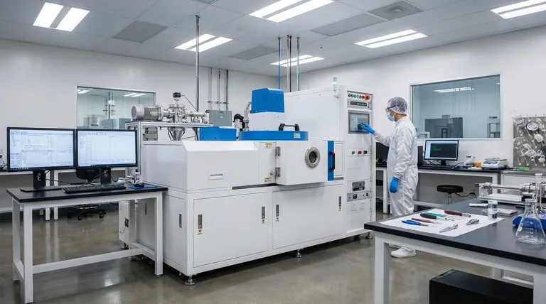
The primary physical methods for thin film deposition are categorized under the umbrella of Physical Vapor Deposition (PVD). These techniques involve physically transferring material from a source to a substrate in a vacuum, most commonly through either sputtering or evaporation. Unlike chemical methods, PVD does not rely on chemical reactions to form the film, offering a direct path to creating high-purity coatings.
The crucial distinction between physical deposition methods is not which is universally "better," but how each one's unique mechanism—energetic bombardment versus gentle condensation—aligns with your specific material, substrate, and desired film properties.
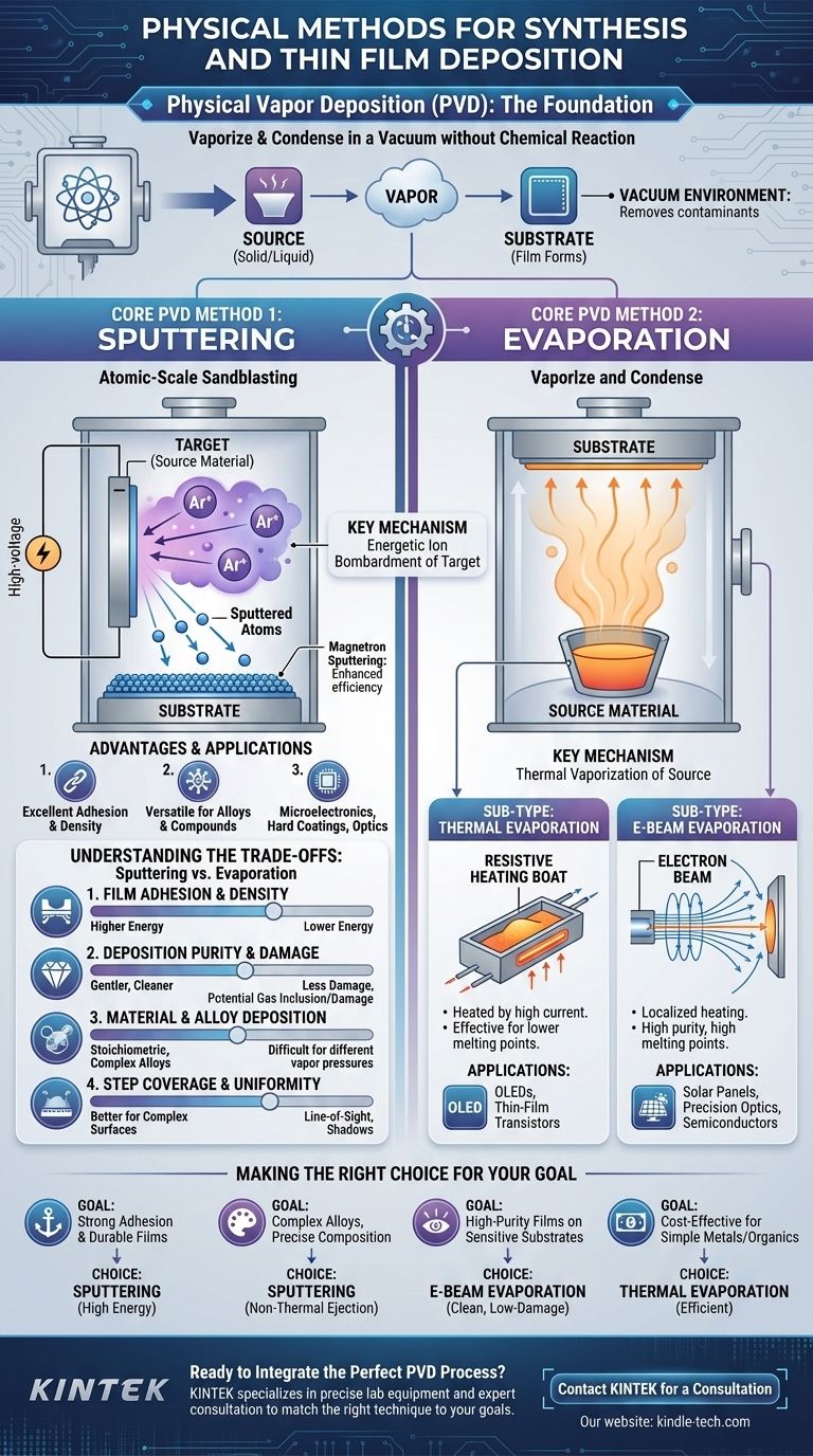
The Foundation: What is Physical Vapor Deposition (PVD)?
Physical Vapor Deposition encompasses a family of processes where a solid or liquid source material is converted into a vapor and transported to a substrate, where it condenses to form a thin film.
The Defining Principle
All PVD processes occur in a vacuum chamber. This environment is critical because it removes atmospheric gases that could react with the vapor or impede its path to the substrate.
The core of PVD is a purely physical mechanism. Material is dislodged from a source (known as a "target") and travels to the substrate without undergoing a deliberate chemical change. This is the key difference from methods like Chemical Vapor Deposition (CVD), which uses precursor gases that react to form the film.
Core PVD Method 1: Sputtering
Sputtering is an incredibly versatile and widely used PVD technique, known for creating dense, durable, and strongly adhered films.
The Sputtering Process Explained
Think of sputtering as an atomic-scale sandblasting process. A high voltage is applied in the vacuum chamber, creating a plasma from an inert gas like Argon.
These energized gas ions are accelerated and bombarded into the source material target. The impact has enough energy to knock out, or "sputter," individual atoms from the target. These ejected atoms then travel through the vacuum and deposit onto the substrate, building up the thin film layer by layer.
Key Advantages and Applications
Sputtering is highly valued for its versatility and scalability. It can deposit a vast range of materials, including metals, alloys, and even insulating compounds (when using a variant called RF sputtering).
Its ability to produce uniform coatings over large areas makes it a cornerstone of industries producing optical coatings, hard protective layers on tools, and the conductive layers in microelectronics. Magnetron sputtering, a common enhancement, uses magnetic fields to increase deposition rates and efficiency.
Core PVD Method 2: Evaporation
Evaporation is a conceptually simpler PVD method that relies on heating a material until it transforms into a vapor that can condense onto a substrate.
The Evaporation Process Explained
Inside the vacuum chamber, the source material is heated until its vapor pressure becomes high enough for atoms to leave its surface and travel outwards.
This vapor then travels in a straight line until it hits the cooler substrate, where it condenses back into a solid state, forming the thin film. The method of heating defines the two primary sub-types.
Sub-Type: Thermal Evaporation
In thermal evaporation, the source material is placed in a small, electrically resistive crucible or "boat" (often made of tungsten or molybdenum). A high current is passed through this boat, heating it and the source material to the point of evaporation.
This method is particularly effective for materials with lower melting points and is a standard process for depositing metals and creating the layers in OLEDs and some thin-film transistors.
Sub-Type: Electron-Beam (E-Beam) Evaporation
For materials with very high melting points, E-beam evaporation is used. A high-energy beam of electrons is generated and magnetically steered to strike the source material.
The intense energy from the electron beam melts and evaporates a localized spot on the source material. This is a cleaner process that allows for higher deposition rates and produces high-purity films, making it ideal for precision optics, solar panels, and semiconductor applications.
Understanding the Trade-offs: Sputtering vs. Evaporation
Choosing the right physical method requires understanding their inherent differences in energy, material handling, and film quality.
Film Adhesion and Density
Sputtering wins here. Sputtered atoms arrive at the substrate with significantly higher kinetic energy than evaporated atoms. This energy helps them form a denser, more compact film with superior adhesion to the substrate.
Deposition Purity and Substrate Damage
Evaporation is generally gentler. Because it's a lower-energy process, evaporation introduces less stress and potential heat damage to sensitive substrates. E-beam evaporation, in particular, is known for creating extremely high-purity films. Sputtering, due to the plasma and ion bombardment, can sometimes embed inert gas atoms into the film or cause minor radiation damage.
Material and Alloy Deposition
Sputtering is more versatile. It can deposit alloys and compounds while preserving their original composition, as the sputtering process ejects atoms stoichiometrically. In evaporation, materials with different vapor pressures can evaporate at different rates, making it difficult to maintain the correct composition for complex alloys.
Step Coverage and Uniformity
Sputtering provides more uniform coverage over complex, non-flat surfaces. The sputtered atoms scatter more within the chamber, allowing them to coat the sides of features. Evaporation is a "line-of-sight" process, which can create "shadows" and poor coverage on intricate topographies.
Making the Right Choice for Your Goal
Selecting a physical deposition method is an exercise in matching the process capabilities to your desired outcome.
- If your primary focus is strong adhesion and durable films: Sputtering is the superior choice due to the higher energy of the depositing particles.
- If your primary focus is depositing complex alloys with precise composition: Sputtering's non-thermal ejection mechanism makes it the most reliable option.
- If your primary focus is high-purity films on sensitive substrates: E-beam evaporation provides a clean, low-damage process ideal for precision optical and electronic applications.
- If your primary focus is cost-effective deposition of simple metals or organics: Thermal evaporation is a well-established and efficient technique for applications like OLEDs.
Ultimately, understanding the fundamental physics of each method empowers you to select the tool that will most effectively and efficiently achieve your goal.
Summary Table:
| Method | Key Mechanism | Key Advantages | Common Applications |
|---|---|---|---|
| Sputtering | Energetic ion bombardment of a target | Excellent adhesion, dense films, versatile for alloys | Microelectronics, hard protective coatings, optics |
| Evaporation | Thermal vaporization of a source material | High-purity films, gentle on sensitive substrates | OLEDs, solar panels, precision optics |
| Thermal Evaporation | Heating with a resistive boat | Cost-effective for simple metals | OLEDs, thin-film transistors |
| E-Beam Evaporation | Heating with a focused electron beam | High purity, high melting point materials | Semiconductors, solar panels, precision optics |
Ready to Integrate the Perfect PVD Process into Your Lab?
Choosing between sputtering and evaporation is critical for achieving your desired film properties, from adhesion and purity to composition and uniformity. KINTEK specializes in providing the precise lab equipment and expert consultation to match the right PVD technique to your specific research and production goals.
We help laboratories like yours enhance efficiency and achieve reliable, high-quality results. Contact us today to discuss your thin film deposition needs and discover how our solutions can advance your work.
Contact KINTEK for a Consultation
Visual Guide
Related Products
- Aluminized Ceramic Evaporation Boat for Thin Film Deposition
- Tungsten Evaporation Boat for Thin Film Deposition
- Electron Beam Evaporation Coating Oxygen-Free Copper Crucible and Evaporation Boat
- Molybdenum Tungsten Tantalum Evaporation Boat for High Temperature Applications
- HFCVD Machine System Equipment for Drawing Die Nano-Diamond Coating
People Also Ask
- What is the widely used boat made of in thermal evaporation? Choosing the Right Material for High-Purity Deposition
- What are the alternatives to sputtering? Choose the Right Thin Film Deposition Method
- What are the applications of thin films deposition? Unlock New Possibilities for Your Materials
- Why is an alumina boat selected for catalyst precursors? Ensure Sample Purity at 1000 °C
- Why is an alumina boat and Ti3AlC2 powder bed necessary for Ti2AlC sintering? Protect MAX Phase Purity


