In essence, physical methods of thin film deposition are processes that use mechanical, thermal, or electromechanical means to transfer a material from a source to a substrate inside a vacuum. The two most common physical vapor deposition (PVD) techniques are sputtering, which ejects material by bombarding a source with energetic ions, and thermal evaporation, which heats a material until it vaporizes. Other key physical methods include pulsed laser deposition (PLD) and molecular beam epitaxy (MBE).
The core distinction between physical deposition methods is not which is "best," but how they create a vapor from a solid source. Your choice depends on a fundamental trade-off between deposition speed, film quality, material complexity, and cost, with each method offering a unique balance of these factors.
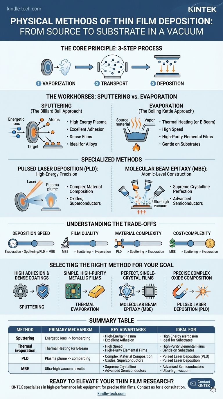
The Core Principle: From Solid to Vapor to Film
All physical deposition techniques share a common three-step process, which occurs in a vacuum to ensure purity and control. Understanding this sequence is key to grasping how they differ.
The Three Foundational Steps
- Vaporization: A solid source material (the "target") is converted into a vapor phase. This is the primary step where techniques diverge—some boil the material, others knock atoms loose.
- Transport: The vaporized atoms or molecules travel through the vacuum chamber from the source to the substrate. The vacuum ensures they don't collide with air molecules.
- Deposition: The vapor condenses onto the cooler substrate, forming a solid thin film layer by layer.
The Workhorses of PVD: Sputtering vs. Evaporation
While many physical methods exist, sputtering and evaporation are the most widely used in both research and industrial production. They represent two fundamentally different approaches to the vaporization step.
Sputtering: The Billiard Ball Approach
Sputtering uses a high-energy plasma to generate ions (typically from an inert gas like Argon). These ions are accelerated into a target made of the desired deposition material.
The impact is like a subatomic game of billiards: the energetic ions physically knock atoms loose from the target's surface. These "sputtered" atoms then travel across the chamber and deposit onto the substrate.
Sputtering provides excellent film adhesion and can create dense, uniform films. It is exceptionally well-suited for depositing alloys and complex compounds because it tends to preserve the material's original composition (stoichiometry).
Evaporation: The Boiling Kettle Approach
Thermal evaporation is conceptually simpler. The source material is placed in a container (a "boat" or crucible) inside a vacuum chamber and heated until it begins to boil and evaporate.
This vapor then rises, travels through the vacuum, and condenses on the substrate, much like steam condensing on a cool surface. A more advanced version, Electron Beam Evaporation, uses a high-energy electron beam to heat the source material, allowing for higher deposition temperatures and purer films.
Evaporation is often faster and gentler on the substrate than sputtering. It is a highly effective method for depositing high-purity elemental films, such as metals for electrical contacts.
Specialized Physical Deposition Methods
Beyond the two mainstays, specialized techniques offer unique capabilities for cutting-edge applications, often prioritizing ultimate precision over speed or cost.
Pulsed Laser Deposition (PLD): High-Energy Precision
In PLD, a high-power pulsed laser is focused on the target material inside the vacuum chamber. Each laser pulse is so energetic that it instantly ablates (vaporizes) a tiny amount of the source material, creating a plume of plasma that deposits onto the substrate.
PLD's key advantage is its ability to faithfully transfer the composition of complex, multi-element materials (like high-temperature superconductors or specific oxides) from the target to the film.
Molecular Beam Epitaxy (MBE): Atomic-Level Construction
MBE is the pinnacle of deposition control. In an ultra-high vacuum environment, highly pure elemental sources are heated in specialized effusion cells, creating low-flux "molecular beams."
These beams are aimed at a pristine, heated single-crystal substrate. The deposition rate is extremely slow—often less than one atomic layer per second—allowing atoms to arrange themselves perfectly into the substrate's crystal lattice. This produces the highest quality single-crystal epitaxial films, which are the foundation of many advanced semiconductor devices.
Understanding the Trade-offs
Choosing a physical deposition method requires a clear understanding of its inherent compromises. There is no single best technique; there is only the right technique for your specific application.
Film Quality vs. Deposition Rate
Sputtered films are typically dense, adherent, and durable. MBE produces films with unparalleled crystalline perfection. However, both methods are generally slower than thermal evaporation, which can deposit material very quickly but may result in less dense films.
Material Compatibility
Evaporation is limited by a material's melting point and vapor pressure. Sputtering can deposit nearly any material, including refractory metals and insulators, making it highly versatile. PLD shines specifically with complex oxides that are difficult to manage with other methods.
Energy and Substrate Damage
Sputtering is a high-energy, physical bombardment process. This energy improves film adhesion but can also induce stress or damage in sensitive substrates. Evaporation is a much lower-energy process, making it a "gentler" choice for delicate electronics or organic materials.
System Complexity and Cost
Thermal evaporators are relatively simple and low-cost. Sputtering systems are more complex due to the need for plasma generation and power supplies. MBE systems are by far the most complex and expensive, requiring ultra-high vacuum and precise in-situ monitoring tools.
Selecting the Right Physical Method for Your Goal
Your choice should be driven by the final properties you need your thin film to have.
- If your primary focus is high adhesion and dense coatings for mechanical or optical use: Sputtering is almost always the superior choice due to the energetic deposition process.
- If your primary focus is simple, cost-effective, high-purity metallic films for electronics: Thermal Evaporation offers an excellent balance of speed, simplicity, and film quality.
- If your primary focus is perfect, single-crystal films for advanced semiconductors or quantum devices: Molecular Beam Epitaxy (MBE) is the undisputed standard for achieving atomic-level perfection.
- If your primary focus is preserving the exact composition of a complex oxide or superconductor: Pulsed Laser Deposition (PLD) provides the most reliable way to transfer stoichiometry from target to substrate.
Understanding these core principles and trade-offs empowers you to select the physical deposition method that precisely matches your material, budget, and performance requirements.
Summary Table:
| Method | Primary Vaporization Mechanism | Key Advantages | Ideal For |
|---|---|---|---|
| Sputtering | Energetic ion bombardment | Excellent adhesion, dense films, handles alloys/compounds | Mechanical/optical coatings, complex materials |
| Thermal Evaporation | Heating to vaporize | High speed, high-purity elemental films, gentle on substrates | Simple metallic films (e.g., electrical contacts) |
| Pulsed Laser Deposition (PLD) | High-power laser ablation | Preserves complex material stoichiometry | Complex oxides, superconductors |
| Molecular Beam Epitaxy (MBE) | Thermal effusion in ultra-high vacuum | Atomic-level control, supreme crystalline perfection | Advanced semiconductors, quantum devices |
Ready to Elevate Your Thin Film Research or Production?
Choosing the right deposition method is critical to your project's success. The experts at KINTEK specialize in providing high-performance lab equipment, including sputtering systems, thermal evaporators, and more, tailored to your specific material and application needs.
We help laboratories achieve precise, reliable, and high-quality thin films. Let us guide you to the optimal solution for your budget and performance goals.
Contact KINTEK today for a personalized consultation and discover how our expertise in lab equipment can accelerate your innovations!
Visual Guide
Related Products
- Chemical Vapor Deposition CVD Equipment System Chamber Slide PECVD Tube Furnace with Liquid Gasifier PECVD Machine
- RF PECVD System Radio Frequency Plasma-Enhanced Chemical Vapor Deposition RF PECVD
- 915MHz MPCVD Diamond Machine Microwave Plasma Chemical Vapor Deposition System Reactor
- HFCVD Machine System Equipment for Drawing Die Nano-Diamond Coating
- Split Chamber CVD Tube Furnace with Vacuum Station Chemical Vapor Deposition System Equipment Machine
People Also Ask
- What types of substrates are used in CVD to facilitate graphene films? Optimize Graphene Growth with the Right Catalyst
- How are carbon nanotubes grown? Master Scalable Production with Chemical Vapor Deposition
- How expensive is chemical vapor deposition? Understanding the True Cost of High-Performance Coating
- What are the processes of vapor phase deposition? Understand CVD vs. PVD for Superior Thin Films
- What is the chemical vapor deposition growth process? Build Superior Thin Films from the Atom Up


