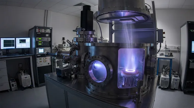
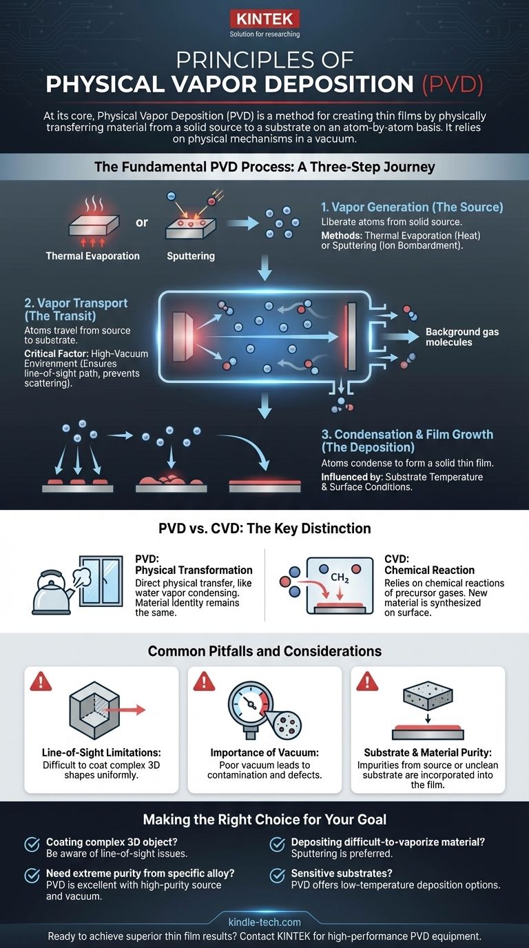
At its core, Physical Vapor Deposition (PVD) is a method for creating thin films by physically transferring material from a solid source to a substrate on an atom-by-atom basis. This process occurs within a vacuum and relies on purely physical mechanisms—like heating or bombardment—to turn solid material into a vapor, which then condenses onto the target surface to form the film. Unlike chemical methods, no fundamental chemical reactions occur to create the final material.
The central principle of PVD is a physical phase transformation: a solid material is converted into a gaseous vapor, transported through a vacuum, and condensed back into a thin solid film on a substrate. It is a direct physical transfer, not a chemical synthesis.
The Fundamental PVD Process: A Three-Step Journey
All PVD techniques, from evaporation to sputtering, are governed by the same three fundamental steps. Understanding this sequence is key to understanding the entire process.
Step 1: Vapor Generation (The Source)
The first step is to create a vapor from the solid source material you wish to deposit. This is achieved by imparting enough energy to the source atoms to liberate them from their solid state.
The two primary methods for this are thermal evaporation (heating the material until it boils or sublimates) and sputtering (bombarding the source with high-energy ions, which physically ejects atoms from the surface).
Step 2: Vapor Transport (The Transit)
Once liberated, the atoms or molecules travel from the source to the substrate. This transport phase must occur in a high-vacuum environment.
A vacuum is critical because it removes other gas molecules (like air) that could collide with and scatter the vapor atoms. This ensures a "line-of-sight" path from the source to the substrate, leading to a more uniform and pure film.
Step 3: Condensation and Film Growth (The Deposition)
When the vapor atoms arrive at the substrate—which is typically kept at a lower temperature—they lose energy and condense back into a solid state.
This condensation does not happen all at once. Atoms nucleate at various points on the surface, forming "islands" that grow and merge until a continuous thin film is formed. The final properties of this film are highly dependent on the deposition conditions.
PVD vs. Chemical Vapor Deposition (CVD): The Key Distinction
The principles of PVD are best understood when contrasted with its chemical counterpart, Chemical Vapor Deposition (CVD). The difference is fundamental.
PVD: A Physical Transformation
As established, PVD is a physical process. Think of it like water vapor from a kettle condensing on a cold window. The material (water) doesn't change its chemical identity; it only changes its physical state from gas to liquid. PVD operates on this same principle, but with solid materials changing from solid to vapor and back to solid.
CVD: A Chemical Reaction
CVD, by contrast, relies on chemical reactions. In this process, one or more reactive precursor gases are introduced into a chamber. These gases react at the substrate's surface, and the solid product of that reaction is the thin film. A new material is synthesized directly on the surface.
Common Pitfalls and Considerations
The physical nature of PVD creates distinct advantages and limitations that are critical to understand for successful application.
Line-of-Sight Limitations
Because the vapor travels in a straight line from the source, PVD is a directional, line-of-sight process. This makes it difficult to uniformly coat complex, three-dimensional shapes with undercuts or hidden surfaces.
The Importance of a Vacuum
The quality of the PVD film is directly tied to the quality of the vacuum. A poor vacuum can lead to contamination from residual gases, resulting in films with poor adhesion, altered properties, and defects. Achieving and maintaining a high vacuum is a primary operational challenge.
Substrate and Material Purity
The PVD process faithfully transfers the source material to the substrate. This means any impurities in the source material will be incorporated into the final film. Likewise, the substrate surface must be exceptionally clean to ensure proper film adhesion and growth.
Making the Right Choice for Your Goal
Understanding these core principles allows you to align the PVD process with your specific technical goals.
- If your primary focus is coating a complex 3D object uniformly: Be aware of PVD's line-of-sight limitations and consider substrate rotation or alternative methods like CVD.
- If your primary focus is creating an extremely pure film from a specific alloy: PVD is an excellent choice, provided you use a high-purity source material and maintain a high-quality vacuum.
- If your primary focus is depositing a material that cannot be easily vaporized: Sputtering is often preferred over thermal evaporation, as it can physically eject atoms from virtually any solid material.
- If your primary focus is low-temperature deposition for sensitive substrates: PVD is often advantageous because, unlike many CVD processes, it can be performed at relatively low temperatures.
Ultimately, mastering thin film deposition begins with recognizing that PVD is fundamentally a process of controlled physical relocation.
Summary Table:
| Principle Step | Key Action | Critical Factor |
|---|---|---|
| 1. Vapor Generation | Liberate atoms from solid source (evaporation/sputtering) | Energy input method (thermal or kinetic) |
| 2. Vapor Transport | Atoms travel from source to substrate | High-vacuum environment (line-of-sight path) |
| 3. Condensation & Film Growth | Atoms condense and form a solid thin film | Substrate temperature and surface conditions |
Ready to achieve superior thin film results in your lab? KINTEK specializes in high-performance PVD equipment and consumables, delivering the precision and purity your research demands. Our experts can help you select the ideal system for your specific materials and substrates. Contact our team today to discuss your PVD needs and elevate your coating capabilities!
Visual Guide
Related Products
- Chemical Vapor Deposition CVD Equipment System Chamber Slide PECVD Tube Furnace with Liquid Gasifier PECVD Machine
- RF PECVD System Radio Frequency Plasma-Enhanced Chemical Vapor Deposition RF PECVD
- Customer Made Versatile CVD Tube Furnace Chemical Vapor Deposition Chamber System Equipment
- Microwave Plasma Chemical Vapor Deposition MPCVD Machine System Reactor for Lab and Diamond Growth
- Custom CVD Diamond Coating for Lab Applications
People Also Ask
- How expensive is chemical vapor deposition? Understanding the True Cost of High-Performance Coating
- What are the processes of vapor phase deposition? Understand CVD vs. PVD for Superior Thin Films
- What is the chemical vapor deposition growth process? Build Superior Thin Films from the Atom Up
- What are the core advantages of PE-CVD in OLED encapsulation? Protect Sensitive Layers with Low-Temp Film Deposition
- What types of substrates are used in CVD to facilitate graphene films? Optimize Graphene Growth with the Right Catalyst


