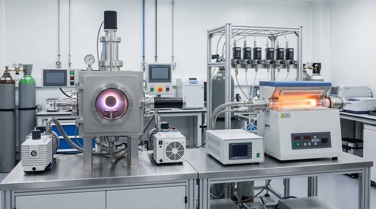
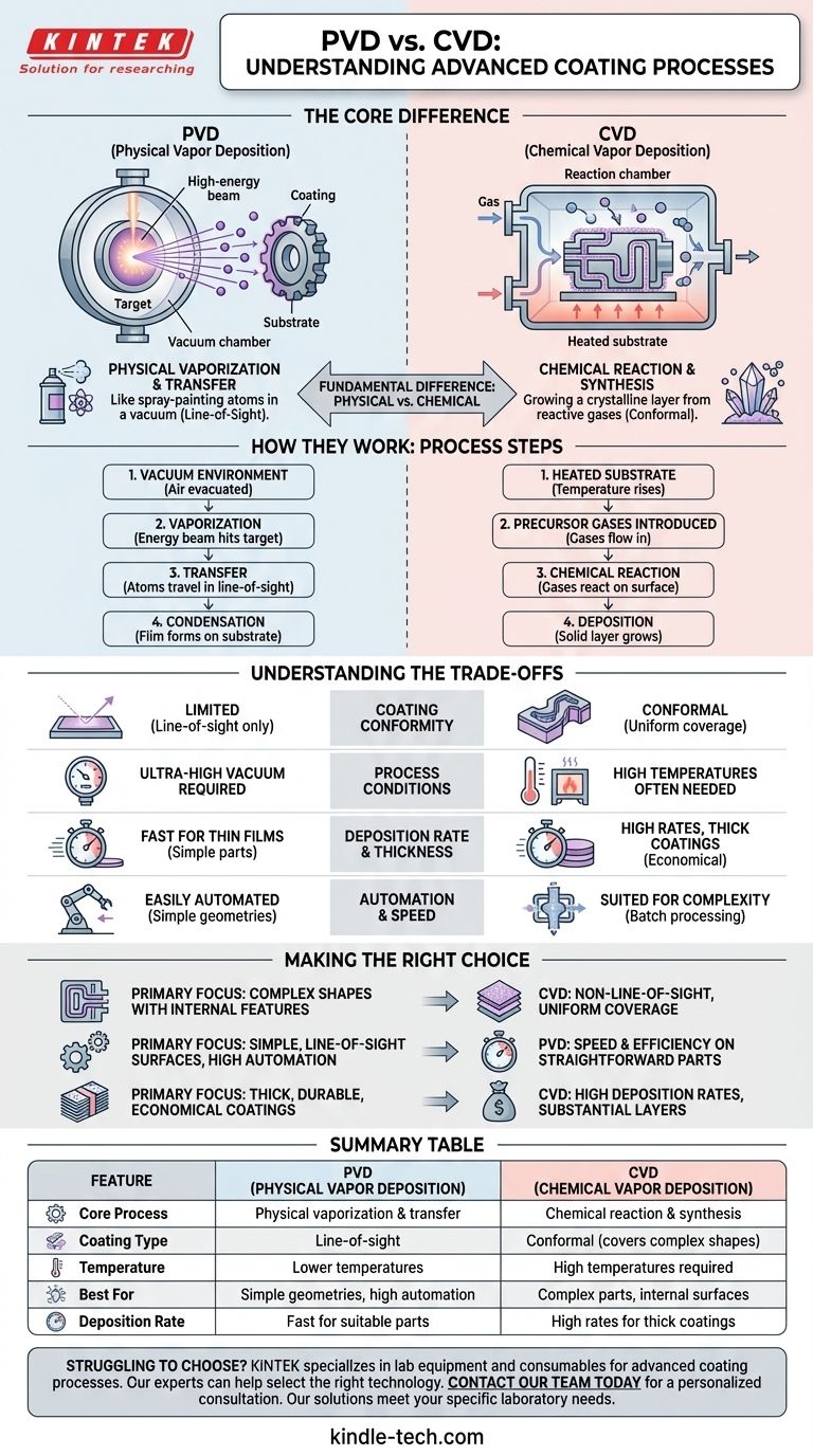
The core difference is that Physical Vapor Deposition (PVD) is a physical process that vaporizes and deposits an existing material onto a surface, while Chemical Vapor Deposition (CVD) is a chemical process that uses gas-phase reactions to create a new material directly on the surface. Both are advanced techniques used to apply very thin, high-performance coatings to tools, molds, and other components.
The simplest way to think about the distinction is that PVD is like spray-painting with atoms in a vacuum, while CVD is like growing a crystalline layer on a surface from a reactive gas. This fundamental difference dictates which process is suitable for a given application.
How Physical Vapor Deposition (PVD) Works
PVD encompasses a set of vacuum deposition methods used to produce thin films and coatings. The process is fundamentally a physical transfer of material from a source to a substrate.
The Core Principle: Vaporization and Condensation
At its heart, PVD takes a solid or liquid source material (the "target") and turns it into a vapor. This vapor then travels through a vacuum and condenses onto the part you want to coat (the "substrate").
The Basic Process Steps
- A substrate is placed in a vacuum chamber, and the air is evacuated to create a high-vacuum environment.
- A high-energy source, such as a high-voltage power supply or a focused beam, is aimed at the target material.
- This energy vaporizes atoms from the target, which then travel in a straight line through the vacuum chamber.
- The vaporized atoms strike the cooler substrate and condense, forming a thin, tightly bonded film on its surface.
Key Characteristic: Line-of-Sight Deposition
Because the vaporized atoms travel in straight lines, PVD is a line-of-sight process. It can only coat surfaces that have a direct, unobstructed path to the source material, similar to how a spray can only paint what it is aimed at.
How Chemical Vapor Deposition (CVD) Works
CVD creates a coating through a fundamentally different mechanism. Instead of transferring an existing material, it synthesizes the coating material directly on the substrate's surface through a controlled chemical reaction.
The Core Principle: A Controlled Chemical Reaction
CVD involves introducing one or more precursor gases into a reaction chamber. When these gases come into contact with the heated substrate, they react and decompose, forming a solid material that deposits onto the surface.
The Basic Process Steps
- The substrate is placed inside a reaction chamber and heated to a specific temperature.
- Volatile precursor gases are introduced into the chamber.
- The heat energizes the gases, causing them to react or decompose on and around the substrate.
- This chemical reaction produces the desired solid coating material, which "grows" on the substrate's surface.
- Gaseous byproducts from the reaction are exhausted from the chamber.
Key Characteristic: Conformal Coating
Because the precursor gases can flow and diffuse into any open space, CVD is not limited by line-of-sight. It can uniformly coat complex shapes, deep recesses, holes, and internal surfaces with high "throwing power," resulting in a highly conformal layer.
Understanding the Trade-offs
The choice between PVD and CVD depends entirely on the application's requirements, as their distinct mechanisms create critical trade-offs.
Coating Conformity
CVD's primary advantage is its ability to create a uniform coating on parts with complex geometries. PVD struggles with this, often leaving internal channels or the backside of features uncoated.
Process Conditions
PVD typically requires an ultra-high vacuum to allow atoms to travel freely. CVD does not always require this level of vacuum but often operates at very high temperatures to drive the chemical reactions.
Deposition Rate and Thickness
CVD can often achieve high deposition rates and is well-suited for producing very thick coatings economically. While PVD can be very fast for certain applications, CVD is frequently the preferred method for building substantial coating layers.
Automation and Speed
For simpler, line-of-sight components, PVD processes can sometimes be faster and more easily automated than their CVD counterparts, making them highly efficient for high-volume production of suitable parts.
Making the Right Choice for Your Application
Understanding the core mechanism of each process is the key to selecting the correct one for your technical goal.
- If your primary focus is coating complex shapes with internal features: CVD is the superior choice due to its non-line-of-sight deposition, which ensures complete and uniform coverage.
- If your primary focus is coating simple, line-of-sight surfaces and requires high automation: PVD is often preferred for its speed and efficiency on components with straightforward geometries.
- If your primary focus is creating thick, durable, and economical coatings: CVD frequently has an advantage due to its high deposition rates and ability to build substantial material layers.
Ultimately, choosing the right deposition technology depends on a clear understanding of your component's geometry and desired coating properties.
Summary Table:
| Feature | PVD (Physical Vapor Deposition) | CVD (Chemical Vapor Deposition) |
|---|---|---|
| Core Process | Physical vaporization & transfer | Chemical reaction & synthesis |
| Coating Type | Line-of-sight | Conformal (covers complex shapes) |
| Temperature | Lower temperatures | High temperatures required |
| Best For | Simple geometries, high automation | Complex parts, internal surfaces |
| Deposition Rate | Fast for suitable parts | High rates for thick coatings |
Struggling to choose between PVD and CVD for your application? KINTEK specializes in lab equipment and consumables for advanced coating processes. Our experts can help you select the right technology to enhance your component performance, improve durability, and optimize your production efficiency. Contact our team today for a personalized consultation and discover how our solutions can meet your specific laboratory needs.
Visual Guide
Related Products
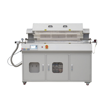
- Chemical Vapor Deposition CVD Equipment System Chamber Slide PECVD Tube Furnace with Liquid Gasifier PECVD Machine
- Inclined Rotary Plasma Enhanced Chemical Vapor Deposition PECVD Equipment Tube Furnace Machine
- RF PECVD System Radio Frequency Plasma-Enhanced Chemical Vapor Deposition RF PECVD
- Customer Made Versatile CVD Tube Furnace Chemical Vapor Deposition Chamber System Equipment
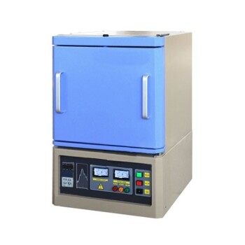
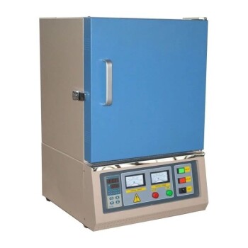
- Vacuum Hot Press Furnace Machine for Lamination and Heating
People Also Ask
- How are PECVD and CVD different? A Guide to Choosing the Right Thin-Film Deposition Process
- Why is PECVD better than CVD? Achieve Superior Low-Temperature Thin Film Deposition
- What is the difference between thermal CVD and PECVD? Choose the Right Thin-Film Deposition Method
- What is the precursor gas in PECVD? The Key to Low-Temperature Thin Film Deposition
- How is PECVD different from CVD? Unlock Low-Temperature Thin Film Deposition