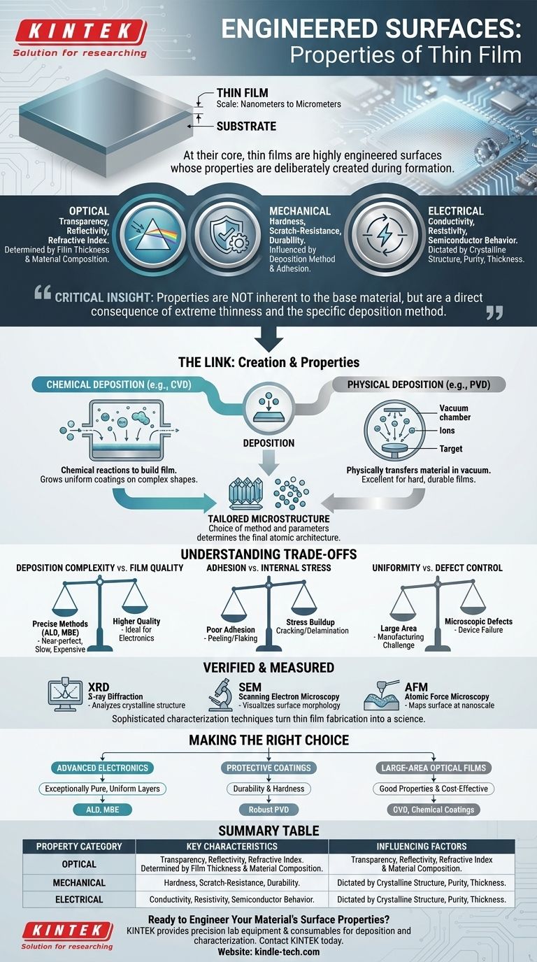
At their core, thin films are not just thin layers of material; they are highly engineered surfaces whose properties are deliberately created during their formation. These properties can be optical (like transparency), mechanical (like scratch-resistance and durability), or electrical (modifying conductivity), all determined by the film's precise thickness and atomic structure.
The most critical insight is that a thin film's properties are not inherent to its base material alone. Instead, they are a direct consequence of its extreme thinness and the specific deposition method used to create it, allowing for the engineering of material characteristics that do not exist in bulk form.
What Fundamentally Defines a Thin Film?
A thin film is a layer of material deposited onto a surface, known as a substrate. Its defining characteristic is its scale, where one dimension (thickness) is dramatically smaller than the other two.
The Scale: From Nanometers to Micrometers
A thin film's thickness can range from a single layer of atoms (a monolayer) to several micrometers. This extreme thinness suppresses the material's three-dimensional properties, causing it to behave more like a two-dimensional surface with unique physical and chemical behaviors.
The Substrate: A Critical Foundation
The film is always attached to a substrate, which can be glass, silicon, metal, or plastic. The interaction between the film and the substrate is crucial, affecting adhesion, internal stress, and the film's final crystalline structure.
The Link Between Creation and Properties
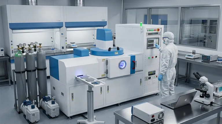
You cannot separate a thin film's properties from its creation process. The method of deposition—how the film is grown or applied—directly controls its final structure and, therefore, its function. Deposition techniques fall into two main categories.
Chemical Deposition Methods
These methods use chemical reactions to build a film on the substrate's surface. In Chemical Vapor Deposition (CVD), precursor gases react in a chamber to form a solid film, "growing" it onto the surface. This allows for uniform coatings over complex shapes.
Physical Deposition Methods
These methods physically transfer material onto the substrate, typically in a vacuum. Physical Vapor Deposition (PVD) includes techniques like sputtering, where ions bombard a target material, ejecting atoms that then coat the substrate. This process is excellent for creating very hard, durable films.
The Result: A Tailored Microstructure
The choice of deposition method and its parameters (temperature, pressure, etc.) determines the film's microstructure—whether its atoms are arranged in an orderly crystal lattice or a disordered, amorphous state. This atomic-level architecture is what ultimately dictates the film's final properties.
Understanding the Trade-offs
While powerful, thin film technology involves significant engineering challenges and compromises. Understanding these trade-offs is key to successful application.
Deposition Complexity vs. Film Quality
The most precise deposition methods, like Atomic Layer Deposition (ALD) or Molecular Beam Epitaxy (MBE), offer atom-by-atom control, resulting in near-perfect films. However, these processes are extremely slow and expensive, making them suitable for high-value applications like microprocessors but impractical for coating large areas.
Adhesion and Internal Stress
A mismatch between the film and the substrate can cause poor adhesion, leading to peeling or flaking. Furthermore, stresses can build up within the film during deposition, causing it to crack or delaminate over time, which compromises its durability and function.
Uniformity and Defect Control
Achieving a perfectly uniform film thickness and a defect-free surface across a large area (like a display screen or solar panel) is a major manufacturing challenge. Even microscopic defects can lead to device failure, especially in electronics.
How Properties Are Verified and Measured
The properties of a thin film are not assumed; they are precisely measured using sophisticated characterization techniques. This verification step is what turns thin film fabrication from an art into a science.
Analyzing Crystalline Structure
Techniques like X-ray Diffraction (XRD) are used to analyze the atomic arrangement within the film. This tells us whether the film is crystalline or amorphous, which is a primary determinant of its electrical and optical behavior.
Visualizing the Surface and Morphology
Microscopy is essential for seeing the film's structure. Scanning Electron Microscopy (SEM) provides high-magnification images of the surface topography, while Atomic Force Microscopy (AFM) can map the surface with nanoscale resolution, revealing its smoothness and grain structure.
Making the Right Choice for Your Application
The ideal thin film is entirely dependent on the problem you need to solve. Your goal dictates the required properties, which in turn points to the most suitable fabrication method.
- If your primary focus is advanced electronics: You need exceptionally pure, uniform layers with precise thickness control, making methods like ALD or MBE the necessary choice.
- If your primary focus is protective coatings: Durability and hardness are paramount, meaning robust PVD methods like sputtering are often the most effective and economical solution.
- If your primary focus is large-area optical films: You need good optical properties and cost-effectiveness over a large surface, making methods like CVD or various chemical coating techniques highly suitable.
Ultimately, the power of thin films lies in the precise control over their fabrication, allowing us to engineer material properties at the nanoscale to meet specific technological demands.
Summary Table:
| Property Category | Key Characteristics | Influencing Factors |
|---|---|---|
| Optical | Transparency, Reflectivity, Refractive Index | Film Thickness, Material Composition |
| Mechanical | Hardness, Scratch-Resistance, Durability | Deposition Method, Adhesion to Substrate |
| Electrical | Conductivity, Resistivity, Semiconductor Behavior | Crystalline Structure, Purity, Thickness |
Ready to Engineer Your Material's Surface Properties?
Whether you're developing advanced electronics, durable protective coatings, or high-performance optical films, KINTEK provides the precision lab equipment and consumables you need. Our expertise in deposition systems and characterization tools helps you achieve the exact thin film properties required for your application.
Contact KINTEK today to discuss your project and discover how our solutions can accelerate your innovation in thin film technology.
Visual Guide
Related Products
- Aluminum-Plastic Flexible Packaging Film for Lithium Battery Packaging
- Thin-Layer Spectral Electrolysis Electrochemical Cell
People Also Ask
- What are the properties of Aluminium (Al) relevant to its use in coatings? High Reflectivity & Conductivity Explored
- What is the difference between single layer film and multi layer film? A Guide to Material Selection
- What is the difference between monolayer and multilayer film? Choose the Right Packaging for Your Product
- What are the three types of lamination? Choose the Perfect Finish for Your Print Project
- What is the thinnest coating? Unlocking Unique Properties at the Atomic Scale

