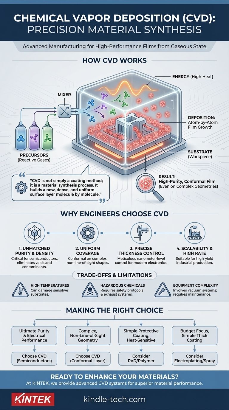
At its core, chemical vapor deposition (CVD) is an advanced manufacturing process used to grow a solid, high-performance film onto a surface from a gaseous state. It functions by introducing reactive gases, known as precursors, into a chamber containing the object to be coated (the substrate). An energy source then triggers a chemical reaction, causing the gases to decompose and deposit a new, ultra-pure solid layer onto the substrate's surface.
The crucial insight is that CVD is not simply a coating method; it is a material synthesis process. It builds a new, dense, and uniform surface layer molecule by molecule, enabling the creation of materials and functionalities that are impossible with conventional techniques.
How Chemical Vapor Deposition Fundamentally Works
To understand what makes CVD so powerful, you must look at its core mechanism. It’s a precise, controlled sequence that transforms gas into a high-purity solid.
The Core Components: Substrate, Precursors, and Energy
The process hinges on three key elements. The substrate is the workpiece or part that receives the new layer. The precursors are carefully selected volatile gases that contain the atoms needed for the final film. Finally, energy—typically in the form of high heat—is introduced to initiate the chemical reaction.
The Step-by-Step Process in the Chamber
A substrate is placed inside a sealed reaction chamber, which is often a vacuum to remove contaminants. The precursor gases are then flowed into the chamber at a controlled rate. When these gases reach the heated substrate, the thermal energy breaks them down, causing the desired atoms to deposit and bond with the surface, building the film one atomic layer at a time.
The Result: A High-Purity, Conformal Film
Because the deposition happens from a gaseous phase, the process is non-line-of-sight. Think of it like how dew forms evenly on every surface of a complex plant, even the undersides of leaves. CVD creates an exceptionally uniform, or conformal, coating that covers even the most intricate geometries and internal surfaces perfectly. The resulting film is also extremely pure, as the process is sealed from outside contaminants.
Why Engineers Choose CVD
Engineers and scientists don't choose CVD just for a simple protective layer; they choose it when performance and precision are non-negotiable.
Unmatched Purity and Density
CVD produces films with very high purity and density. This is critical in applications like semiconductors, where even microscopic impurities can cause a device to fail. The process builds the material from the atom up, eliminating voids and contaminants found in other methods.
Uniform Coverage on Complex Shapes
For components with complex internal channels, holes, or intricate surface features, CVD is often the only viable option. Line-of-sight processes like spray painting or physical vapor deposition (PVD) cannot reach these areas, but the precursor gases in CVD can, ensuring complete and uniform coverage.
Precise Control Over Ultra-Thin Layers
The process allows for meticulous control over the film's thickness, down to the level of nanometers. This makes it indispensable for modern electronics, where the electrical properties of a device are determined by the thickness of its ultra-thin layers.
High Deposition Rates and Scalability
While incredibly precise, CVD can also deposit material at a relatively high rate compared to other atomic-level processes. This combination of speed and precision makes it suitable for high-yield manufacturing and is relatively simple to scale up for industrial production.
Understanding the Trade-offs and Limitations
No process is perfect. True expertise requires understanding the limitations and potential downsides of CVD.
High Temperatures Can Limit Substrate Choice
Traditional CVD processes often require very high temperatures (over 600°C) to trigger the chemical reactions. This heat can damage or warp temperature-sensitive substrates, such as plastics or certain metal alloys, limiting its application for those materials.
Precursor Chemicals Can Be Hazardous
The precursor gases used in CVD are often toxic, flammable, or corrosive. This necessitates sophisticated safety protocols, handling equipment, and exhaust management systems, which can add to the complexity and cost of the operation.
Equipment Complexity and Maintenance
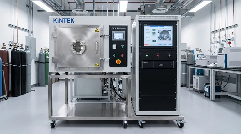
A CVD reactor is a complex piece of equipment involving vacuum systems, precise gas flow controllers, and high-temperature components. These parts, such as the heating filaments mentioned in Hot-Filament CVD (HFCVD), can degrade over time and require regular maintenance or replacement, leading to operational downtime.
Making the Right Choice for Your Application
Selecting a manufacturing process depends entirely on your end goal. Use these points as a guide.
- If your primary focus is ultimate purity and electrical performance: CVD is the industry standard for manufacturing semiconductors and advanced optical components for this reason.
- If your primary focus is coating a complex, non-line-of-sight geometry: CVD's ability to create a conformal layer is its defining advantage and is likely your best choice.
- If your primary focus is a simple protective coating on a heat-sensitive part: A lower-temperature process like PVD or even a simple polymer coating may be a more practical and cost-effective solution.
- If your primary focus is budget and you only need a thick, simple coating: Less sophisticated methods like electroplating or spray coating are almost always cheaper and faster for non-critical applications.
Ultimately, chemical vapor deposition empowers engineers to build new surfaces with precisely controlled properties, making it a foundational technology for virtually all modern high-performance materials.
Summary Table:
| CVD Characteristic | Key Advantage |
|---|---|
| Process Type | Vapor-phase material synthesis |
| Film Quality | High purity and density |
| Coverage | Conformal, non-line-of-sight |
| Thickness Control | Nanometer precision |
| Ideal For | Semiconductors, complex geometries, high-performance coatings |
| Common Limitation | High process temperatures |
Ready to enhance your materials with precision coatings?
At KINTEK, we specialize in providing advanced lab equipment, including CVD systems, to help you achieve superior material performance. Whether you're developing next-generation semiconductors or need durable coatings for complex components, our solutions deliver the purity and uniformity your research demands.
Let's discuss how our expertise can support your project. Contact our team today for a personalized consultation.
Visual Guide
Related Products
- Chemical Vapor Deposition CVD Equipment System Chamber Slide PECVD Tube Furnace with Liquid Gasifier PECVD Machine
- Microwave Plasma Chemical Vapor Deposition MPCVD Machine System Reactor for Lab and Diamond Growth
- 915MHz MPCVD Diamond Machine Microwave Plasma Chemical Vapor Deposition System Reactor
- Customer Made Versatile CVD Tube Furnace Chemical Vapor Deposition Chamber System Equipment
- HFCVD Machine System Equipment for Drawing Die Nano-Diamond Coating
People Also Ask
- What happens during deposition chemistry? Building Thin Films from Gaseous Precursors
- What are the processes of vapor phase deposition? Understand CVD vs. PVD for Superior Thin Films
- What are the advantages of chemical vapor deposition? Achieve Superior Thin Films for Your Lab
- What are the core advantages of PE-CVD in OLED encapsulation? Protect Sensitive Layers with Low-Temp Film Deposition
- What is the chemical vapor deposition growth process? Build Superior Thin Films from the Atom Up


