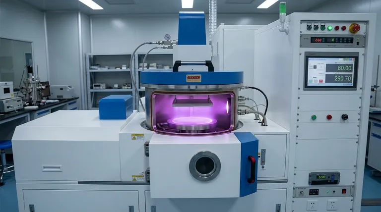
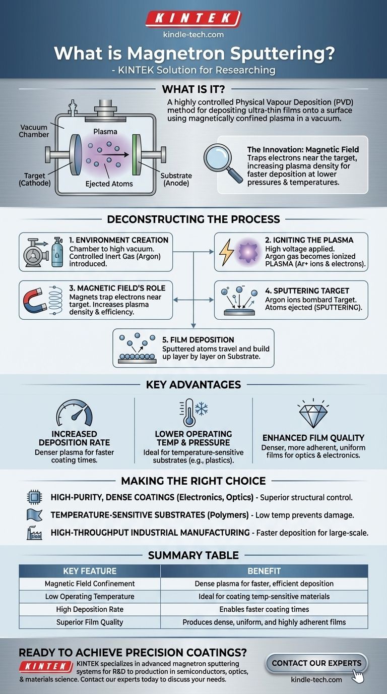
At its core, magnetron sputtering is a highly controlled method for depositing ultra-thin films of material onto a surface. It is a type of Physical Vapour Deposition (PVD) that operates within a vacuum and uses a magnetically confined plasma. This plasma bombards a source material, known as a 'target', causing its atoms to be ejected and subsequently coat a desired object, or 'substrate', with remarkable precision.
The critical innovation of magnetron sputtering is not the sputtering itself, but the strategic use of a magnetic field. This field traps electrons near the target material, dramatically increasing the plasma's density and efficiency, which allows for faster deposition rates at lower pressures and temperatures.
Deconstructing the Magnetron Sputtering Process
To understand how this technology creates high-quality thin films, it's best to break it down into its fundamental steps. The entire process takes place within a high-vacuum chamber.
Step 1: Creating the Environment
First, the chamber is pumped down to a high vacuum to remove any contaminants. A small, controlled amount of an inert gas, typically argon, is then introduced into the chamber at a very low pressure.
Step 2: Igniting the Plasma
A high voltage is applied across the chamber, with the target material acting as the negatively charged cathode. This electric field energizes the argon gas, stripping electrons from the argon atoms and creating a plasma—a glowing, ionized gas composed of positive argon ions and free electrons.
Step 3: The Role of the Magnetic Field
This is the "magnetron" component. A powerful magnetic field is strategically placed behind the target. This field traps the lighter, negatively charged electrons, forcing them into a spiral path close to the target's surface.
This electron trap is the key. By keeping electrons near the target, it drastically increases the probability that they will collide with and ionize more argon atoms, creating a much denser and more sustainable plasma right where it's needed most.
Step 4: Sputtering the Target
The heavy, positively charged argon ions in the plasma are not significantly affected by the magnetic field. They are accelerated by the electric field and violently collide with the negatively charged target material.
Each impact has enough energy to knock atoms loose from the target's surface in a process known as sputtering. These liberated atoms are ejected into the vacuum environment.
Step 5: Film Deposition
The sputtered atoms from the target travel through the vacuum chamber and land on the substrate (the object to be coated). As these atoms accumulate, they condense and build up layer by layer, forming a thin, uniform, and highly pure film.
Understanding the Trade-offs and Key Advantages
The use of a magnetic field is not an arbitrary addition; it is a fundamental improvement over simple sputtering techniques that provides significant, measurable benefits.
Increased Deposition Rate
The dense plasma created by the magnetic confinement leads to a much higher rate of ion bombardment on the target. This results in more sputtered atoms per second, allowing films to be deposited much faster than in non-magnetron systems.
Lower Operating Pressure and Temperature
Because the magnetic field makes the plasma so efficient, the process can be sustained at lower gas pressures. Furthermore, by trapping electrons at the target, it prevents them from bombarding and heating the substrate, making it ideal for coating temperature-sensitive materials like plastics.
Enhanced Film Quality
The high-density plasma and energetic atom bombardment generally result in films that are denser, more adherent, and have better uniformity compared to other methods. This is critical for applications in optics and semiconductors.
Making the Right Choice for Your Goal
Magnetron sputtering is an exceptionally versatile and powerful tool, but its suitability depends entirely on the required outcome.
- If your primary focus is high-purity, dense coatings for electronics or optics: Magnetron sputtering offers superior control over film structure and adhesion.
- If your primary focus is coating temperature-sensitive substrates like polymers: The low operating temperature of this process is a critical advantage that prevents substrate damage.
- If your primary focus is high-throughput industrial manufacturing: The significantly faster deposition rates make it a more economically viable choice for large-scale production.
Ultimately, choosing magnetron sputtering is a decision for precision, efficiency, and quality in thin-film deposition.
Summary Table:
| Key Feature | Benefit |
|---|---|
| Magnetic Field Confinement | Creates a dense plasma for faster, more efficient deposition |
| Low Operating Temperature | Ideal for coating temperature-sensitive materials (e.g., plastics) |
| High Deposition Rate | Enables faster coating times for industrial throughput |
| Superior Film Quality | Produces dense, uniform, and highly adherent thin films |
Ready to achieve precision coatings for your lab?
KINTEK specializes in advanced lab equipment, including magnetron sputtering systems designed for researchers and manufacturers in semiconductors, optics, and materials science. Our solutions deliver the high-quality, uniform thin films your projects demand, with the efficiency to scale from R&D to production.
Contact our experts today to discuss how a KINTEK sputtering system can enhance your capabilities and accelerate your innovation.
Visual Guide
Related Products
- Spark Plasma Sintering Furnace SPS Furnace
- RF PECVD System Radio Frequency Plasma-Enhanced Chemical Vapor Deposition RF PECVD
People Also Ask
- What is SPS sintering method? A Guide to High-Speed, High-Performance Material Fabrication
- What is the mechanism of SPS process? A Deep Dive into Rapid, Low-Temperature Sintering
- What technical advantages does a Spark Plasma Sintering (SPS) furnace offer for LZP ceramics? Enhance Ionic Conductivity
- What is the difference between spark plasma sintering and flash sintering? A Guide to Advanced Sintering Methods
- What are the advantages of CAMI/SPS for W-Cu composite preparation? Reduce cycles from hours to seconds.

