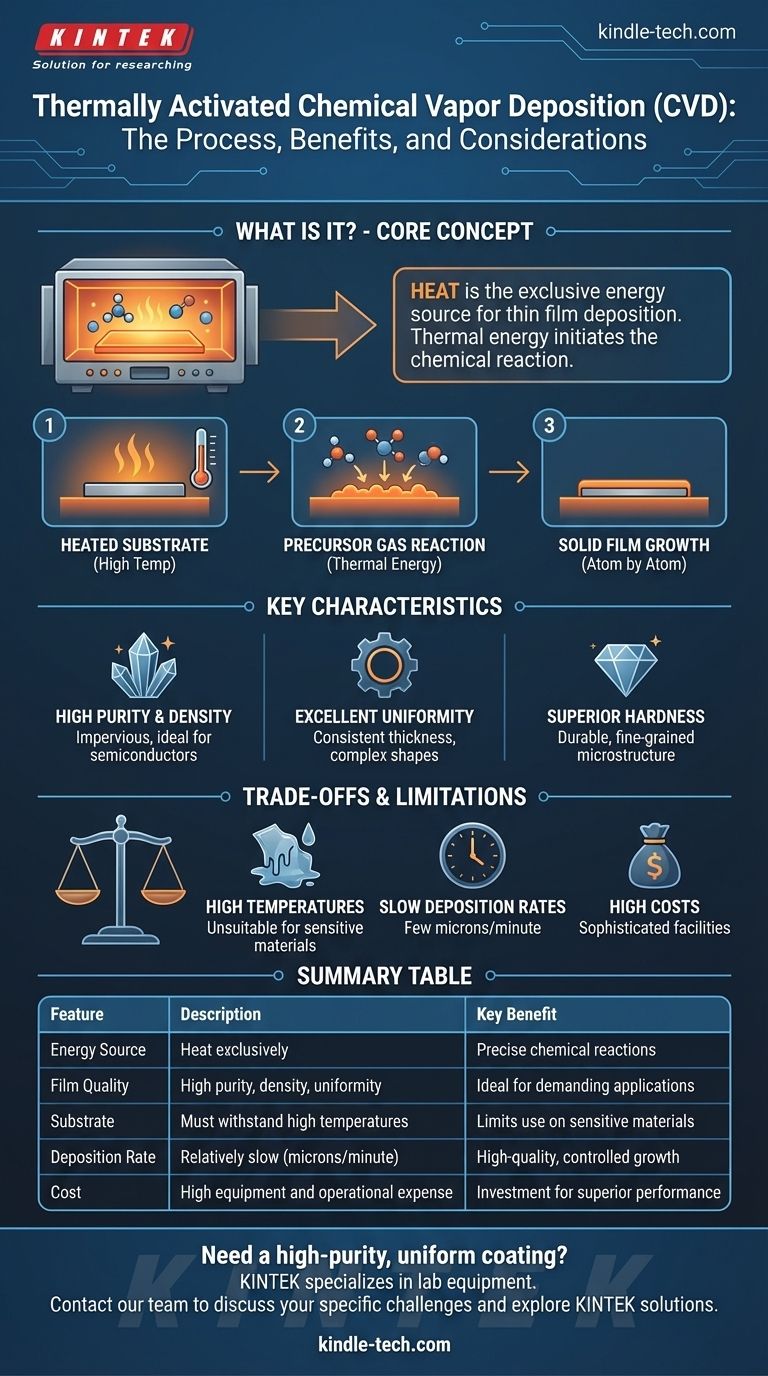
Thermally activated Chemical Vapor Deposition (CVD) is the foundational and most common form of the CVD process. The term "thermally activated" simply specifies that heat is the exclusive energy source used to initiate the chemical reaction that deposits a thin film onto a substrate's surface. This process relies on high temperatures to provide the necessary energy for precursor gases to react and form a solid coating.
The core concept to understand is that heat is the engine of this process. In thermally activated CVD, a substrate is heated to a specific temperature, and this thermal energy alone is responsible for breaking down precursor gases and driving the chemical reactions needed to create a high-quality, uniform thin film.
How Thermal Activation Drives the Deposition Process
The entire CVD process is a carefully controlled chemical reaction that happens on a surface, not in a beaker. Heat is the catalyst and primary driver for every step.
The Role of the Heated Substrate
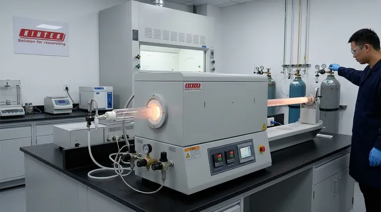
The process begins by heating the object to be coated, known as the substrate, inside a reaction chamber. This is typically done at elevated temperatures, often several hundred degrees Celsius. This heat provides the critical thermal energy required for the deposition reaction to occur.
The Precursor Gas Reaction
Once the substrate reaches the target temperature, one or more reactive gases, known as precursors, are introduced into the chamber. When these gases come into contact with the hot substrate, the thermal energy causes them to decompose and react chemically.
Solid Film Growth
The chemical reaction produces the desired solid material, which then deposits atom by atom onto the hot substrate. This results in the growth of a dense, uniform, and highly pure thin film with a fine-grained structure.
Key Characteristics of Thermally Deposited Films
The quality of a film created by thermally activated CVD is its primary advantage. The controlled, heat-driven reaction leads to coatings with exceptional properties.
High Purity and Density
Because the reaction is purely chemical and occurs in a controlled environment, the resulting films are impervious and have very high purity. This makes them ideal for applications in semiconductors and protective coatings where material integrity is paramount.
Excellent Uniformity
Thermally activated CVD is renowned for its ability to produce coatings of uniform thickness, even over complex shapes. The gaseous nature of the precursors allows them to reach all exposed surfaces of the substrate before reacting.
Superior Hardness
CVD coatings are characteristically harder and more durable than the same materials produced through conventional fabrication methods. This is due to the fine-grained and dense microstructure formed during deposition.
Understanding the Trade-offs and Limitations
While powerful, the reliance on high heat creates specific constraints that are critical to understand before choosing this method.
The Need for High Temperatures
The defining feature of this process is also its main limitation. The substrate must be able to withstand the high temperatures required to activate the chemical reaction. This makes the process unsuitable for temperature-sensitive materials like certain plastics or polymers.
Relatively Slow Deposition Rates
The film growth is precise and controlled, but this often translates to slow deposition rates, typically measured in a few microns per minute. This can lead to long production times for thicker coatings.
High Equipment and Production Costs
Creating and maintaining a high-temperature, controlled-gas environment requires sophisticated and expensive facilities. These high operational and capital costs can make the process less economically viable for some applications.
Making the Right Choice for Your Goal
Ultimately, deciding whether thermally activated CVD is appropriate depends entirely on your project's priorities. The trade-off is almost always between ultimate film quality and production constraints like cost, speed, and substrate compatibility.
- If your primary focus is ultimate film quality, purity, and uniformity: Thermally activated CVD is an excellent choice, delivering coatings that are often superior to those from other methods.
- If your primary focus is depositing on temperature-sensitive substrates: You must explore alternative low-temperature deposition methods, as the high heat required by this process will damage the material.
- If your primary focus is high-volume, low-cost production: The slow deposition rates and high equipment costs of thermal CVD may be prohibitive, suggesting an evaluation of other techniques.
Understanding that the energy source defines the process is the key to selecting the right tool for your engineering challenge.
Summary Table:
| Feature | Description | Key Benefit |
|---|---|---|
| Energy Source | Heat exclusively | Drives precise chemical reactions |
| Film Quality | High purity, density, and uniformity | Ideal for demanding applications |
| Substrate Requirement | Must withstand high temperatures | Limits use on sensitive materials |
| Deposition Rate | Relatively slow (microns/minute) | Ensures high-quality, controlled growth |
| Cost | High equipment and operational expense | Investment for superior performance |
Need a high-purity, uniform coating for your lab's substrates?
Thermally activated CVD delivers exceptional film quality, but its high-temperature requirements and costs need expert guidance. KINTEK specializes in lab equipment and consumables, serving laboratory needs with precision CVD solutions.
Our experts can help you determine if thermal CVD is the right choice for your application and provide the reliable equipment you need for success.
Contact our team today to discuss your specific coating challenges and explore how KINTEK can enhance your lab's capabilities!
Visual Guide
Related Products
- CVD Diamond for Thermal Management Applications
- HFCVD Machine System Equipment for Drawing Die Nano-Diamond Coating
- Multi Heating Zones CVD Tube Furnace Machine Chemical Vapor Deposition Chamber System Equipment
- Microwave Plasma Chemical Vapor Deposition MPCVD Machine System Reactor for Lab and Diamond Growth
- Chemical Vapor Deposition CVD Equipment System Chamber Slide PECVD Tube Furnace with Liquid Gasifier PECVD Machine
People Also Ask
- What are the characteristics of CVD diamond? Unlocking Superior Performance for Industrial Tools
- How long do CVD diamonds last? Discover the Truth About Their Lifespan
- How long does it take to make a CVD diamond? A Detailed Look at the Growth Timeline
- Are CVD diamonds real or fake? Discover the Truth About Lab-Grown Diamonds
- What is the hardness of CVD diamond? The Ultimate Guide to Engineered Super-Materials