In semiconductor manufacturing, Atomic Layer Deposition (ALD) is a process for depositing ultrathin, highly uniform films of material with atomic-level precision. Unlike other methods that deposit material continuously, ALD builds films one single atomic layer at a time through a sequence of self-limiting chemical reactions. This meticulous control is what makes it indispensable for creating modern, high-performance microchips.
The true value of ALD isn't just its ability to create thin films; it's the unparalleled ability to perfectly coat complex, three-dimensional nanoscale structures. This perfect "conformality" solves a critical geometry problem that older deposition methods cannot, enabling the very architecture of advanced transistors.
How ALD Works: A Self-Limiting Cycle
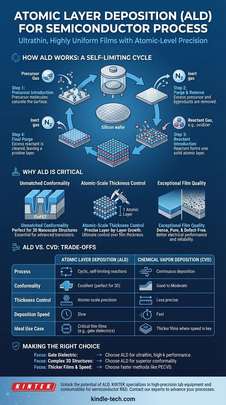
At its core, ALD is a four-step process that repeats to build up a film. The magic lies in its "self-limiting" nature, where each step of the reaction proceeds until it can't go any further, ensuring exactly one atomic layer is added per cycle.
Step 1: Precursor Pulse
A gas containing the first chemical element (the precursor) is introduced into the process chamber. The precursor molecules react with and bond to the surface of the silicon wafer until all available bonding sites are occupied.
Step 2: The First Purge
Once the surface is saturated, any excess precursor molecules and reaction byproducts are completely removed from the chamber using an inert gas, like nitrogen or argon. This step is critical to prevent unwanted reactions in the next phase.
Step 3: Reactant Pulse
A second gas (the reactant, often an oxidizer like water or ozone) is introduced. This reactant chemically reacts with the precursor molecules that are already bonded to the surface, forming a single, solid atomic layer of the desired material.
Step 4: The Final Purge
Finally, any excess reactant gas and byproducts from the second reaction are purged from the chamber. At the end of this step, the wafer is left with a pristine, single atomic layer of new material, ready for the next cycle to begin.
Why ALD is Critical for Modern Semiconductors
The unique cyclic process of ALD provides benefits that are essential for manufacturing chips at nodes of 10nm and below.
Unmatched Conformality
Conformality is the ability of a film to evenly coat a textured surface. Because ALD reactions happen everywhere on the surface, it can deposit a perfectly uniform film over incredibly complex 3D structures, like the vertical fins of a FinFET transistor or the deep trenches of a DRAM capacitor. Other methods, like Physical Vapor Deposition (PVD), are line-of-sight and cannot coat sidewalls or bottoms effectively.
Atomic-Scale Thickness Control
Since each cycle deposits a single, predictable atomic layer, engineers have ultimate control over the final film thickness. For critical components like gate dielectrics, which may only be a few nanometers thick, this precision is non-negotiable for device performance and reliability.
Exceptional Film Quality
The slow, methodical nature of ALD results in films that are incredibly dense, pure, and free of defects like pinholes. This high quality translates directly to better electrical performance, such as lower current leakage and higher device reliability.
Understanding the Trade-offs: ALD vs. CVD
While powerful, ALD is not the solution for every deposition task. It has one major trade-off that must be considered.
The Primary Drawback: Deposition Speed
ALD is an inherently slow process. The need for four separate steps—two chemical pulses and two long purges—for every single atomic layer makes its deposition rate significantly lower than that of Chemical Vapor Deposition (CVD), which deposits material continuously.
When to Choose Which Method
The choice between ALD and CVD is a classic engineering trade-off between perfection and speed.
ALD is chosen for the most critical, thinnest layers where absolute conformality and precision are required, such as high-k gate dielectrics in logic chips. The superior quality justifies the slow speed and higher cost.
CVD is chosen for thicker films where throughput is more important and perfect uniformity is less critical, such as depositing thick oxide layers for insulation between metal wires.
Making the Right Choice for Your Goal
To select the appropriate deposition technology, you must align the method's strengths with the specific requirements of the film layer.
- If your primary focus is creating the gate dielectric for an advanced transistor: ALD is the only viable choice for depositing the ultrathin, high-k, pinhole-free layer needed for performance.
- If your primary focus is coating a complex 3D structure like a FinFET or a deep trench: ALD's superior conformality is non-negotiable to ensure the device functions correctly.
- If your primary focus is depositing a relatively thick insulating or conductive film where speed is paramount: A faster method like Plasma-Enhanced CVD (PECVD) is almost always the more economical and practical solution.
Ultimately, understanding the role of ALD is understanding the enabling technology that allows chip designers to shrink transistors and build vertically in the third dimension.
Summary Table:
| Feature | Atomic Layer Deposition (ALD) | Chemical Vapor Deposition (CVD) |
|---|---|---|
| Process | Cyclic, self-limiting reactions | Continuous deposition |
| Conformality | Excellent (perfect for 3D structures) | Good to Moderate |
| Thickness Control | Atomic-scale precision | Less precise |
| Deposition Speed | Slow | Fast |
| Ideal Use Case | Critical thin films (e.g., gate dielectrics) | Thicker films where speed is key |
Unlock the potential of Atomic Layer Deposition in your lab. KINTEK specializes in providing high-precision lab equipment and consumables for semiconductor research and development. Whether you are developing next-generation transistors or need reliable tools for thin-film deposition, our expertise ensures you achieve the accuracy and performance your work demands. Contact our experts today to discuss how our solutions can advance your semiconductor processes.
Visual Guide
Related Products
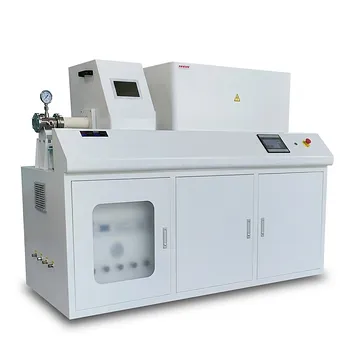
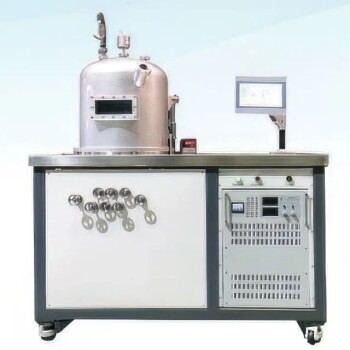
- RF PECVD System Radio Frequency Plasma-Enhanced Chemical Vapor Deposition RF PECVD
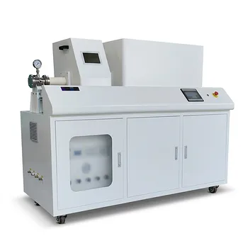
- Chemical Vapor Deposition CVD Equipment System Chamber Slide PECVD Tube Furnace with Liquid Gasifier PECVD Machine
- HFCVD Machine System Equipment for Drawing Die Nano-Diamond Coating
- Aluminized Ceramic Evaporation Boat for Thin Film Deposition
- Inclined Rotary Plasma Enhanced Chemical Vapor Deposition PECVD Equipment Tube Furnace Machine
People Also Ask
- Why is a Matching Network Indispensable in RF-PECVD for Siloxane Films? Ensure Stable Plasma and Uniform Deposition
- What is plasma enhanced chemical vapour deposition PECVD used for? Enable Low-Temp Thin Films for Electronics & Solar
- What is plasma CVD? Unlock Low-Temperature Thin Film Deposition for Sensitive Materials
- What is plasma enhanced chemical Vapour deposition process used for fabrication of? A Guide to Low-Temperature Thin Films
- How does plasma enhance CVD? Unlock Low-Temperature, High-Quality Film Deposition

