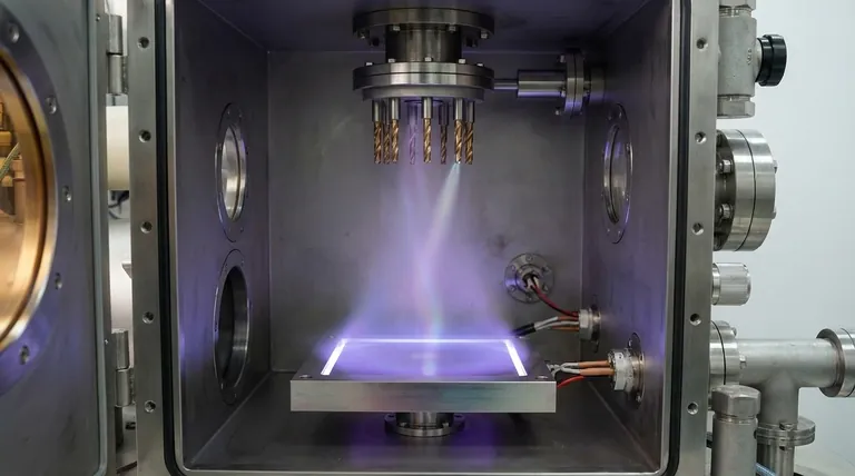
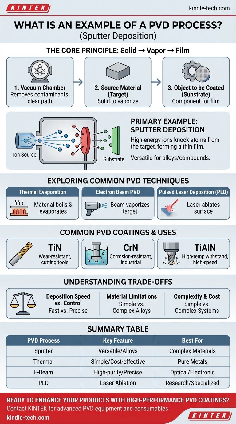
A clear example of a PVD process is sputter deposition. In this technique, a solid block of the coating material, known as the "target," is placed in a vacuum chamber. High-energy ions, typically from an inert gas like argon, are fired at this target, acting like a microscopic sandblaster. This bombardment is energetic enough to knock individual atoms off the target's surface, which then travel through the vacuum and deposit onto the object being coated, forming a thin, uniform film.
All Physical Vapor Deposition (PVD) processes share a core principle: a solid source material is vaporized in a vacuum, transported atom by atom, and then condensed onto a substrate to form a high-performance coating. The specific method of vaporization is what differentiates the techniques.
The Core Principle of PVD: From Solid to Vapor to Film
To understand any PVD process, it's essential to recognize the three fundamental components that are always present, regardless of the specific technique.
The Vacuum Chamber
Every PVD process takes place in a high-vacuum environment. This is critical because it removes air and other contaminants that could react with the vaporized material and compromise the coating's quality.
The vacuum also ensures the vaporized atoms have a clear, unimpeded path from the source material to the object being coated.
The Source Material (The "Target")
This is the solid material you intend to use for the coating. It could be a pure metal like titanium or chromium, or an alloy. This material is what gets turned into a vapor.
The Object to Be Coated (The "Substrate")
This is simply the part or component onto which the thin film will be deposited. Substrates can range from medical implants and cutting tools to architectural hardware and semiconductor wafers.
Exploring Common PVD Techniques
The key difference between PVD methods lies in how they generate the vapor from the solid target material.
Sputter Deposition
As our primary example, sputtering uses ion bombardment to dislodge atoms from the target. It is an extremely versatile process that works with a vast range of materials, including alloys and compounds that are difficult to evaporate.
Thermal Evaporation
This is one of the simplest PVD methods. The source material is heated in the vacuum chamber until it begins to boil and evaporate, much like water creating steam. This metallic vapor then travels and condenses on the cooler substrate.
Electron Beam Deposition (E-Beam PVD)
In this technique, a high-energy beam of electrons is fired at the target material. The intense energy from the beam melts and vaporizes the source material in a very controlled and localized spot, creating a vapor stream that coats the substrate.
Pulsed Laser Deposition (PLD)
PLD uses a high-power laser, fired in short pulses, to ablate the surface of the target. Each laser pulse vaporizes a tiny amount of material, creating a plume of plasma that travels to the substrate and forms the thin film.
Common PVD Coatings and Their Uses
The PVD process is not an end in itself; it is a means to create functional coatings with specific properties.
Titanium Nitride (TiN)
Recognized by its distinct gold color, TiN is extremely hard and wear-resistant. It is commonly applied to cutting tools like drill bits to extend their life, as well as on decorative items like door handles and faucets for a durable, aesthetic finish.
Chromium Nitride (CrN)
CrN offers superior corrosion resistance and is slightly harder than chrome plating. It is often used in industrial applications on components that face corrosive or high-wear environments.
Titanium Aluminum Nitride (TiAlN)
This is a high-performance coating known for its ability to withstand high temperatures. This property makes it ideal for high-speed cutting tools that generate significant heat during operation.
Understanding the Trade-offs
Choosing a PVD process involves balancing complexity, cost, and the desired outcome. No single technique is best for every application.
Deposition Speed vs. Control
Methods like thermal evaporation can be very fast, but it can be harder to maintain precise control over the film's thickness and structure. Techniques like sputter deposition or E-Beam PVD offer much finer control but may have slower deposition rates.
Material Limitations
Thermal evaporation only works for materials that can be readily vaporized by heat without decomposing. Sputtering, on the other hand, can deposit virtually any material, including complex alloys, making it far more versatile.
Equipment Complexity and Cost
Simple thermal evaporators are relatively inexpensive. In contrast, systems for E-Beam PVD or Pulsed Laser Deposition are significantly more complex and costly due to the need for high-power electron guns or lasers.
Matching the Process to Your Goal
Your choice of PVD method ultimately depends on the properties you need in the final coating.
- If your primary focus is versatility and coating complex alloys: Sputter deposition is an excellent choice due to its ability to handle nearly any target material.
- If your primary focus is a simple, cost-effective process for pure metals: Thermal evaporation is often the most straightforward and economical method.
- If your primary focus is achieving very high-purity films with precise control: Electron Beam PVD is a superior technique for creating high-quality optical and electronic coatings.
Understanding this fundamental mechanism of vaporizing and condensing a material empowers you to select the right PVD technique for any application.
Summary Table:
| PVD Process | Key Feature | Best For |
|---|---|---|
| Sputter Deposition | Versatile, works with alloys & compounds | Coating complex materials, high uniformity |
| Thermal Evaporation | Simple, cost-effective | Pure metals, fast deposition |
| Electron Beam PVD | High-purity, precise control | Optical & electronic coatings |
| Pulsed Laser Deposition | Laser ablation for precise films | Research, specialized applications |
Ready to enhance your products with high-performance PVD coatings? KINTEK specializes in advanced lab equipment and consumables for PVD processes, including sputter deposition systems and thermal evaporators. Whether you're coating cutting tools, medical implants, or semiconductor wafers, our solutions deliver durability, precision, and superior performance. Contact us today to discuss your coating needs and discover how KINTEK can optimize your laboratory's capabilities!
Visual Guide
Related Products
- Inclined Rotary Plasma Enhanced Chemical Vapor Deposition PECVD Equipment Tube Furnace Machine
- RF PECVD System Radio Frequency Plasma-Enhanced Chemical Vapor Deposition RF PECVD
- Chemical Vapor Deposition CVD Equipment System Chamber Slide PECVD Tube Furnace with Liquid Gasifier PECVD Machine
- Electron Beam Evaporation Coating Oxygen-Free Copper Crucible and Evaporation Boat
- Microwave Plasma Chemical Vapor Deposition MPCVD Machine System Reactor for Lab and Diamond Growth
People Also Ask
- What is plasma enhanced chemical vapour deposition process? Unlock Low-Temperature, High-Quality Thin Films
- What materials are deposited in PECVD? Discover the Versatile Thin-Film Materials for Your Application
- What is plasma in CVD process? Lowering Deposition Temperatures for Heat-Sensitive Materials
- What is PECVD used for? Achieve Low-Temperature, High-Performance Thin Films
- How does plasma enhanced CVD work? Achieve Low-Temperature, High-Quality Thin Film Deposition