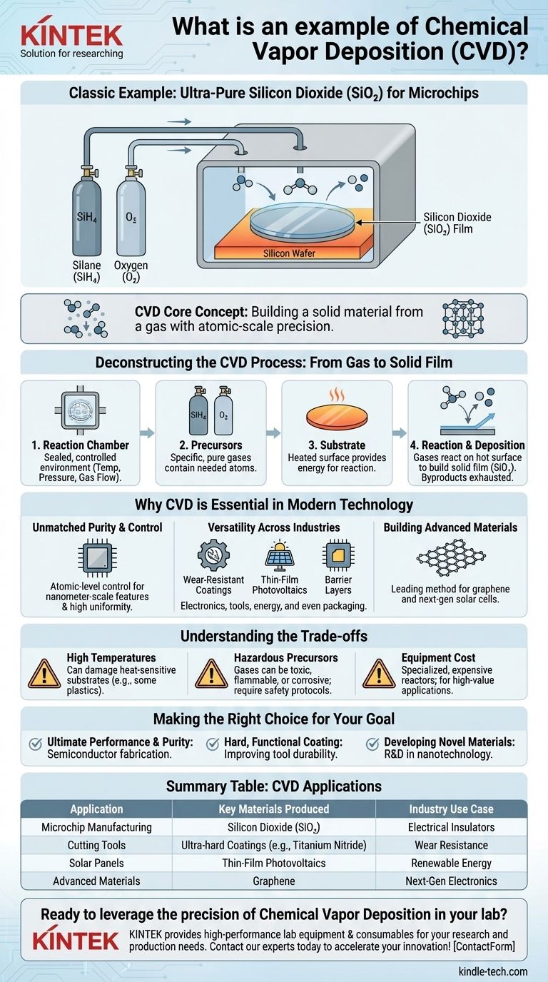
A classic example of chemical vapor deposition (CVD) is the creation of the ultra-pure silicon dioxide (SiO₂) films that act as critical insulators in the manufacturing of every modern microchip. This process involves introducing specific gases, like silane (SiH₄) and oxygen (O₂), into a high-temperature reactor where they chemically react on the surface of a silicon wafer to build a perfect, uniform layer of glass one molecule at a time.
At its core, chemical vapor deposition is a highly controlled method of building a solid material from a gas. Think of it not as painting a surface, but as supplying chemical ingredients in vapor form that react and construct a new, solid film directly on that surface with atomic-scale precision.
Deconstructing the CVD Process: From Gas to Solid Film
To truly understand CVD, let's walk through the example of depositing a silicon dioxide film onto a silicon wafer—a fundamental step in making the transistors that power your phone and computer.
The Reaction Chamber
The entire process takes place inside a sealed, atmosphere-controlled reactor. This chamber allows for precise control over temperature, pressure, and the flow of gases, ensuring no unwanted contaminants interfere with the reaction.
The Gaseous Ingredients (Precursors)
Specific, highly pure gases, known as precursors, are piped into the chamber. In our example, the primary precursors are silane gas (a compound of silicon and hydrogen) and oxygen. These gases contain the atoms needed for the final film (silicon and oxygen).
The Heated Surface (Substrate)
Inside the reactor, the silicon wafer, or substrate, is heated to a high temperature, often several hundred degrees Celsius. This heat is not just for warmth; it provides the critical energy needed to break the chemical bonds in the precursor gases and drive the reaction.
The Chemical Reaction and Deposition
When the precursor gases flow over the hot wafer surface, the thermal energy triggers a chemical reaction. The silane and oxygen molecules react to form solid silicon dioxide (SiO₂), which deposits as a thin, uniform film on the wafer. Gaseous byproducts, such as water vapor, are then exhausted from the chamber.
Why CVD is Essential in Modern Technology
This seemingly complex process is a cornerstone of advanced manufacturing for several key reasons. It offers a level of control that other methods cannot match.
Unmatched Purity and Control
Because the film is built directly from a chemical reaction, the process yields materials with exceptionally high purity and uniformity. This atomic-level control is non-negotiable for creating the nanometer-scale features of a modern semiconductor device.
Versatility Across Industries
While essential for electronics, CVD's applications are incredibly broad. It's used to apply ultra-hard, wear-resistant coatings to cutting tools, create the thin-film photovoltaic layers in solar cells, and even deposit the microscopic barrier layers inside potato chip bags that keep them fresh.
Building Advanced Materials
CVD is at the forefront of materials science research. It is a leading method for producing large, high-quality sheets of graphene and is used to develop next-generation materials like printable solar cells.
Understanding the Trade-offs
Despite its power, CVD is not a universal solution. Its precision comes with specific requirements and limitations that are important to understand.
High Temperature Requirements
Many CVD processes require elevated temperatures. This can prevent its use on substrates that might melt, deform, or be otherwise damaged by the heat, such as many plastics.
Complex and Hazardous Precursors
The precursor gases used in CVD can be toxic, flammable, or corrosive. This necessitates sophisticated safety protocols, handling equipment, and exhaust management systems, adding to operational complexity.
Equipment Cost and Complexity
CVD reactors are highly specialized and expensive pieces of equipment. The investment and expertise required to operate and maintain them mean the process is typically reserved for high-value or high-performance applications.
Making the Right Choice for Your Goal
Understanding when and why to use CVD comes down to the required performance of the final product.
- If your primary focus is ultimate performance and purity: CVD is the industry standard for applications like semiconductor fabrication, where even the tiniest defect can cause failure.
- If your primary focus is creating a hard, functional coating: CVD is an excellent choice for improving the durability and lifespan of tools and mechanical components.
- If your primary focus is developing novel materials: The precise control offered by CVD makes it an indispensable tool for research and development in fields like nanotechnology and advanced electronics.
Ultimately, chemical vapor deposition is a foundational manufacturing process that enables us to build the modern world from the atom up.
Summary Table:
| CVD Application | Key Materials Produced | Industry Use Case |
|---|---|---|
| Microchip Manufacturing | Silicon Dioxide (SiO₂) | Electrical Insulators |
| Cutting Tools | Ultra-hard Coatings (e.g., Titanium Nitride) | Wear Resistance |
| Solar Panels | Thin-Film Photovoltaics | Renewable Energy |
| Advanced Materials | Graphene | Next-Gen Electronics |
Ready to leverage the precision of Chemical Vapor Deposition in your lab? KINTEK specializes in providing high-performance lab equipment and consumables tailored to your research and production needs. Whether you are developing next-generation semiconductors, advanced coatings, or novel nanomaterials, our expertise can help you achieve unparalleled purity and control. Contact our experts today to discuss how our solutions can accelerate your innovation!
Visual Guide
Related Products
- CVD Diamond Dressing Tools for Precision Applications
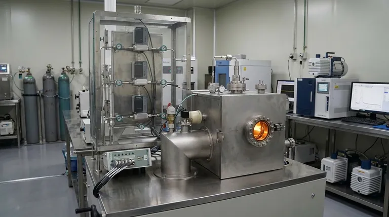
- Multi Heating Zones CVD Tube Furnace Machine Chemical Vapor Deposition Chamber System Equipment
- CVD Diamond Domes for Industrial and Scientific Applications
- CVD Diamond for Thermal Management Applications
- Chemical Vapor Deposition CVD Equipment System Chamber Slide PECVD Tube Furnace with Liquid Gasifier PECVD Machine
People Also Ask
- What color diamonds are CVD? Understanding the Process from Brown Tint to Colorless Beauty
- What is chemical vapor deposition of diamond? Grow High-Purity Diamonds Atom-by-Atom
- Does the chemical vapor deposition be used for diamonds? Yes, for Growing High-Purity Lab Diamonds
- What is CVD diamond? The Ultimate Guide to Lab-Grown Diamonds and Their Uses
- What are the raw materials for CVD diamonds? A seed, a gas, and the science of crystal growth.


