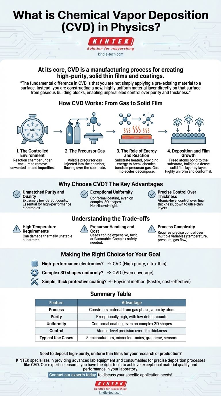
At its core, Chemical Vapor Deposition (CVD) is a manufacturing process for creating high-purity, solid thin films and coatings. It works by introducing a volatile precursor gas into a controlled chamber containing a surface, or substrate. Energy, typically in the form of heat, causes a chemical reaction or decomposition of the gas, allowing the desired material to "deposit" onto the substrate, building a new, solid layer atom by atom.
The fundamental difference in CVD is that you are not simply applying a pre-existing material to a surface. Instead, you are constructing a new, highly uniform material layer directly on that surface from gaseous building blocks, enabling unparalleled control over purity and thickness.
How CVD Works: From Gas to Solid Film
To understand the value of CVD, it's essential to visualize the process not as a simple coating, but as a controlled chemical construction on a molecular scale.
The Controlled Environment
The entire process takes place inside a reaction chamber under vacuum.
The vacuum is critical not to "pull" chemicals, but to remove unwanted air and impurities. This ensures that the only molecules present are those required for the reaction, leading to an exceptionally pure final film.
The Precursor Gas
A "precursor" is a volatile gas that contains the specific atoms you want to deposit. For example, to create a silicon film, you might use silane gas (SiH₄).
This gas is carefully injected into the chamber, where it flows over the component you wish to coat, known as the substrate.
The Role of Energy and Reaction
The substrate is typically heated to a high temperature. This thermal energy provides the catalyst needed to break the chemical bonds in the precursor gas molecules.
When the gas molecules get close to the hot surface, they react or decompose, releasing the atoms needed for the film and forming other gaseous byproducts that are exhausted from the chamber.
Deposition and Film Growth
The freed atoms bond with the substrate's surface. Over time, this process repeats, building up a thin, dense, and solid film layer by layer.
Because the process is driven by a gas that fills the entire chamber, the deposition is highly uniform, or conformal. It evenly coats all exposed surfaces, including complex shapes and internal cavities.
Why Choose CVD? The Key Advantages
Engineers and physicists choose CVD when the properties of the deposited film are more critical than the speed or cost of the process.
Unmatched Purity and Quality
By controlling the input gases precisely, CVD can produce films with extremely low defect counts. This is essential for manufacturing high-performance materials like graphene or the silicon layers in microelectronics.
Exceptional Uniformity
Unlike "line-of-sight" methods like spray painting or physical sputtering, CVD is not directional. The gas precursor surrounds the entire object.
This results in a perfectly even coating, which is critical for components with intricate geometries, ensuring consistent performance across the entire surface.
Precise Control Over Thickness
The film's growth is a direct function of time, temperature, and gas flow. This allows for atomic-level control over the final thickness, making it possible to create the ultra-thin layers required for modern electrical circuits and sensors.
Understanding the Trade-offs
While powerful, CVD is not the solution for every application. Its precision comes with specific requirements and limitations.
High Temperature Requirements
Many CVD processes require very high temperatures to initiate the chemical reaction. This can damage or warp substrates that are not thermally stable, limiting the types of materials that can be coated.
Precursor Handling and Cost
The precursor gases used in CVD can be expensive, highly toxic, corrosive, or flammable. This necessitates complex and costly safety and handling infrastructure.
Process Complexity
Achieving the perfect film requires precise control over multiple variables: temperature, pressure, gas flow rates, and chamber chemistry. This makes the process more complex to set up and run than simpler physical deposition methods.
Making the Right Choice for Your Goal
Selecting a deposition method depends entirely on the required properties of the final product.
- If your primary focus is high-performance electronics or semiconductors: CVD is often the superior choice for its ability to produce highly pure, defect-free, and ultra-thin films.
- If your primary focus is coating complex 3D shapes uniformly: CVD's non-line-of-sight nature ensures even coverage where physical deposition methods would fail.
- If your primary focus is applying a simple, thick protective coating on a heat-resistant material: A simpler physical method might be faster and more cost-effective if extreme purity and uniformity are not critical.
Ultimately, choosing Chemical Vapor Deposition is a decision to prioritize quality, purity, and uniformity in building a material from the ground up.
Summary Table:
| Feature | Advantage |
|---|---|
| Process | Constructs material from gas phase, atom by atom |
| Purity | Exceptionally high, with low defect counts |
| Uniformity | Conformal coating, even on complex 3D shapes |
| Control | Atomic-level precision over film thickness |
| Typical Use Cases | Semiconductors, microelectronics, graphene, sensors |
Need to deposit high-purity, uniform thin films for your research or production? KINTEK specializes in providing advanced lab equipment and consumables for precise deposition processes like CVD. Our expertise ensures you have the right tools to achieve exceptional material quality and performance in your laboratory. Contact our experts today to discuss your specific application needs!
Visual Guide
Related Products
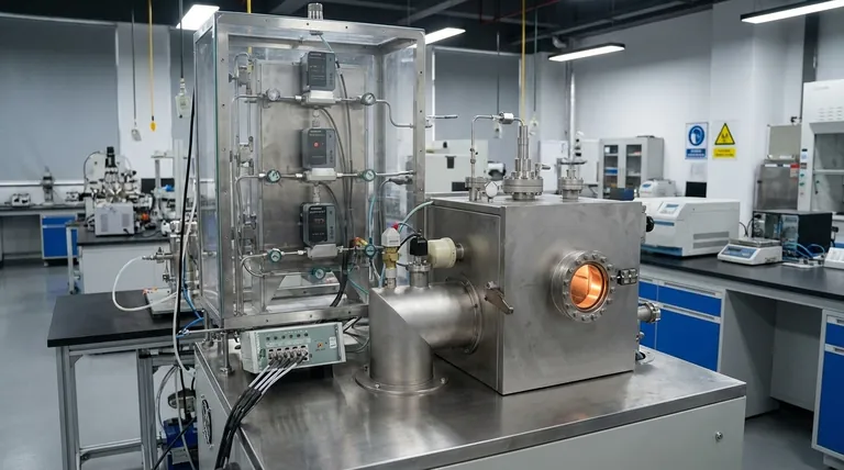
- Chemical Vapor Deposition CVD Equipment System Chamber Slide PECVD Tube Furnace with Liquid Gasifier PECVD Machine
- RF PECVD System Radio Frequency Plasma-Enhanced Chemical Vapor Deposition RF PECVD
- 915MHz MPCVD Diamond Machine Microwave Plasma Chemical Vapor Deposition System Reactor
- Customer Made Versatile CVD Tube Furnace Chemical Vapor Deposition Chamber System Equipment
- Microwave Plasma Chemical Vapor Deposition MPCVD Machine System Reactor for Lab and Diamond Growth
People Also Ask
- Why is Chemical Vapor Deposition (CVD) equipment uniquely suited for constructing hierarchical superhydrophobic structures?
- How expensive is chemical vapor deposition? Understanding the True Cost of High-Performance Coating
- What are the advantages of chemical vapor deposition? Achieve Superior Thin Films for Your Lab
- How are carbon nanotubes grown? Master Scalable Production with Chemical Vapor Deposition
- What types of substrates are used in CVD to facilitate graphene films? Optimize Graphene Growth with the Right Catalyst


