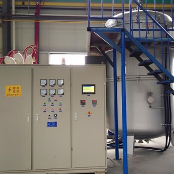
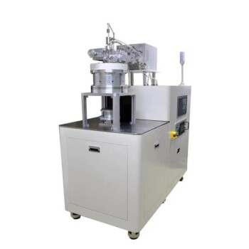
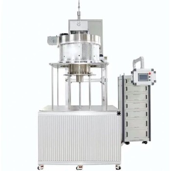
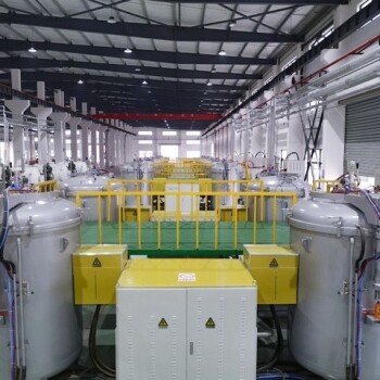
At its core, Chemical Vapor Deposition (CVD) is a method for "growing" a thin film of graphene on a surface. It works by introducing a carbon-containing gas into a high-temperature furnace, causing the gas to decompose and deposit a single layer of carbon atoms onto a catalyst substrate, typically a metal foil like copper or nickel. This technique is currently the most promising and widely used method for producing large-area, high-quality graphene films suitable for industrial and electronic applications.
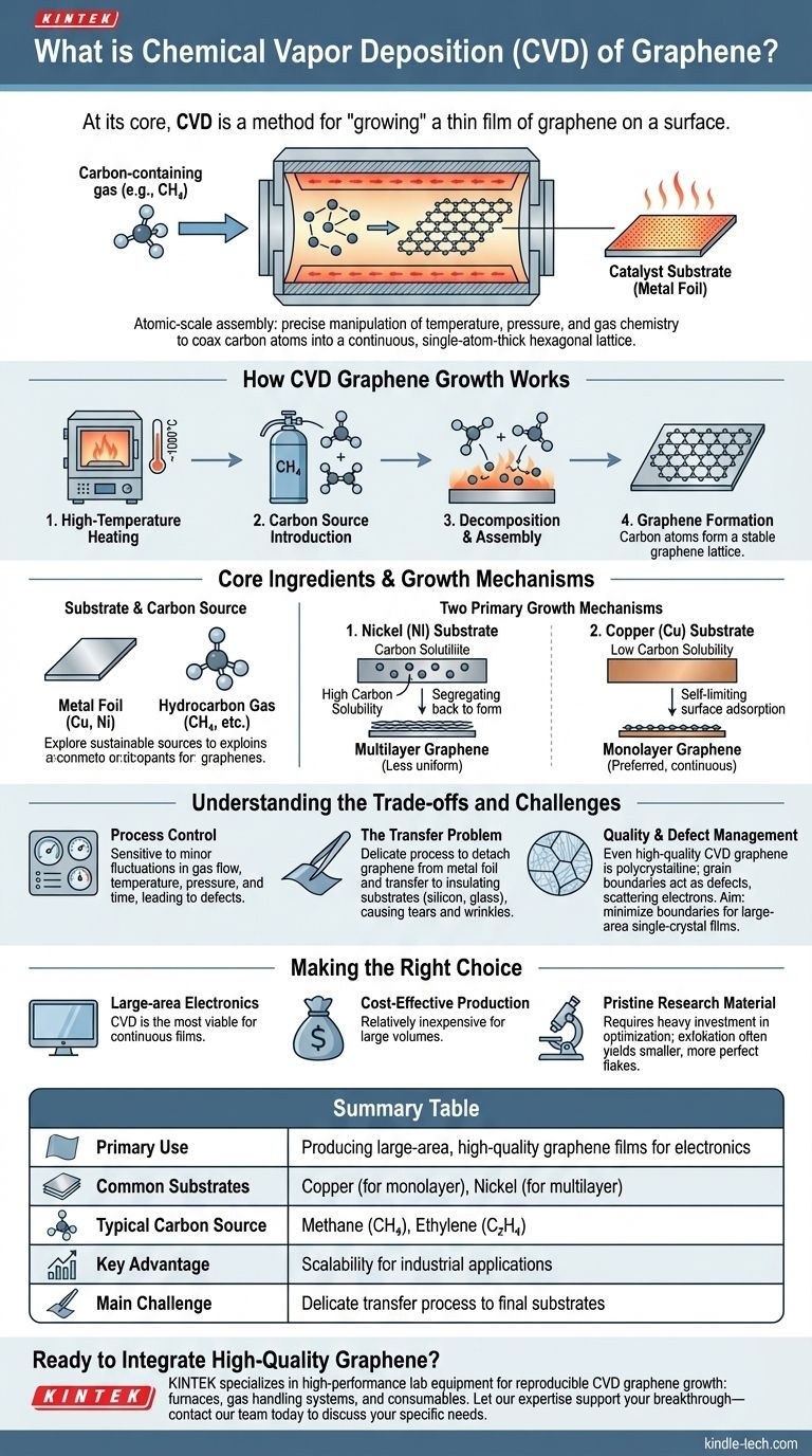
CVD is not a single recipe but a highly controlled process of atomic-scale assembly. Its success hinges on the precise manipulation of temperature, pressure, and gas chemistry to coax carbon atoms into forming a continuous, single-atom-thick hexagonal lattice on a metal surface.
How CVD Graphene Growth Works
To understand CVD, it's best to think of it as a carefully orchestrated chemical reaction occurring on a surface. The process has a few fundamental components and mechanisms.
The Core Ingredients: Substrate and Carbon Source
The process requires two key materials: a growth substrate and a carbon precursor.
The substrate is typically a metal foil that acts as a catalyst for the reaction. Copper (Cu) and Nickel (Ni) are the most common choices.
The carbon precursor is a hydrocarbon gas that will break down to provide the carbon atoms. Common examples include methane (CH₄), ethylene (C₂H₄), or acetylene (C₂H₂). Researchers are also exploring solid and liquid carbon sources, including waste plastics, to make the process more sustainable.
The High-Temperature Reaction
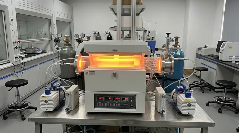
The CVD process unfolds in a controlled sequence within a vacuum furnace:
- The metal substrate is heated to a high temperature, often around 1000°C.
- The carbon-containing gas is introduced into the chamber at a low pressure.
- At this high temperature, the gas molecules decompose on the hot metal surface.
- The freed carbon atoms then rearrange themselves into the stable, honeycomb-like lattice structure of graphene.
Two Primary Growth Mechanisms
The choice of metal substrate fundamentally changes how the graphene film forms.
With a metal like Nickel, which has a high carbon solubility, carbon atoms first dissolve and diffuse into the bulk metal. As the substrate is cooled, the carbon segregates back to the surface to form graphene layers. This can sometimes lead to multiple, less-uniform layers.
With a metal like Copper, which has very low carbon solubility, the process is self-limiting. The graphene grows directly on the surface via adsorption, and once a full layer is formed, the catalytic activity of the surface is shut off. This makes copper the preferred substrate for producing large, continuous monolayer graphene.
Understanding the Trade-offs and Challenges
While CVD is the leading method for scalable production, it is not without its complexities. Achieving high-quality material requires overcoming significant engineering hurdles.
The Critical Role of Process Control
The final quality of the graphene film is exquisitely sensitive to the process parameters. Minor fluctuations in gas flow rates, temperature, pressure, or reaction time can introduce defects, wrinkles, or unwanted multi-layer patches into the film. Producing wafer-scale, single-crystal graphene requires extremely strict process control.
The Transfer Problem
Graphene grown via CVD is on a metal foil, but most applications require it on an insulating substrate like silicon or glass. The film must be carefully detached from the metal and transferred to the new substrate. This transfer process is delicate and a major source of tears, wrinkles, and contamination that can degrade the graphene's exceptional properties.
Quality and Defect Management
Even with excellent control, CVD graphene is polycrystalline, meaning it is made of many small crystal domains stitched together. The boundaries between these domains act as defects that can scatter electrons and weaken the material. Minimizing these grain boundaries to create near-perfect, single-crystal films over large areas remains a primary goal of current research.
Making the Right Choice for Your Goal
Your application dictates whether the advantages of CVD outweigh its challenges. Consider your primary objective when evaluating this technology.
- If your primary focus is large-area electronics or transparent conductors: CVD is the most viable production method, as it is the only technique that reliably produces the large, continuous films required for these applications.
- If your primary focus is cost-effective material production: CVD is relatively inexpensive for large volumes compared to methods like exfoliation, making it the clear choice for industrial scale-up.
- If your primary focus is pristine, defect-free material for fundamental research: While CVD can produce high-quality samples, you must invest heavily in process optimization and characterization, as mechanical exfoliation of graphite often yields smaller but more structurally perfect flakes.
Understanding the principles and inherent trade-offs of CVD is the first step toward harnessing graphene's potential for real-world applications.
Summary Table:
| Aspect | Key Detail |
|---|---|
| Primary Use | Producing large-area, high-quality graphene films for electronics |
| Common Substrates | Copper (for monolayer), Nickel (for multilayer) |
| Typical Carbon Source | Methane (CH₄), Ethylene (C₂H₄) |
| Key Advantage | Scalability for industrial applications |
| Main Challenge | Delicate transfer process to final substrates |
Ready to integrate high-quality graphene into your research or product development? The precise control required for successful CVD graphene growth relies on high-performance lab equipment. KINTEK specializes in the furnaces, gas handling systems, and consumables that laboratories depend on to achieve reproducible results. Let our expertise in lab equipment support your next breakthrough—contact our team today to discuss your specific needs.
Visual Guide
Related Products
- HFCVD Machine System Equipment for Drawing Die Nano-Diamond Coating
- Customer Made Versatile CVD Tube Furnace Chemical Vapor Deposition Chamber System Equipment
- Chemical Vapor Deposition CVD Equipment System Chamber Slide PECVD Tube Furnace with Liquid Gasifier PECVD Machine
- Graphite Vacuum Continuous Graphitization Furnace
- Large Vertical Graphite Vacuum Graphitization Furnace
People Also Ask
- What is the specific function of the metal filament in HF-CVD? Key Roles in Diamond Growth
- What types of substrates are used in CVD to facilitate graphene films? Optimize Graphene Growth with the Right Catalyst
- How expensive is chemical vapor deposition? Understanding the True Cost of High-Performance Coating
- What is the chemical vapor deposition growth process? Build Superior Thin Films from the Atom Up
- What are the advantages of chemical vapor deposition? Achieve Superior Thin Films for Your Lab
