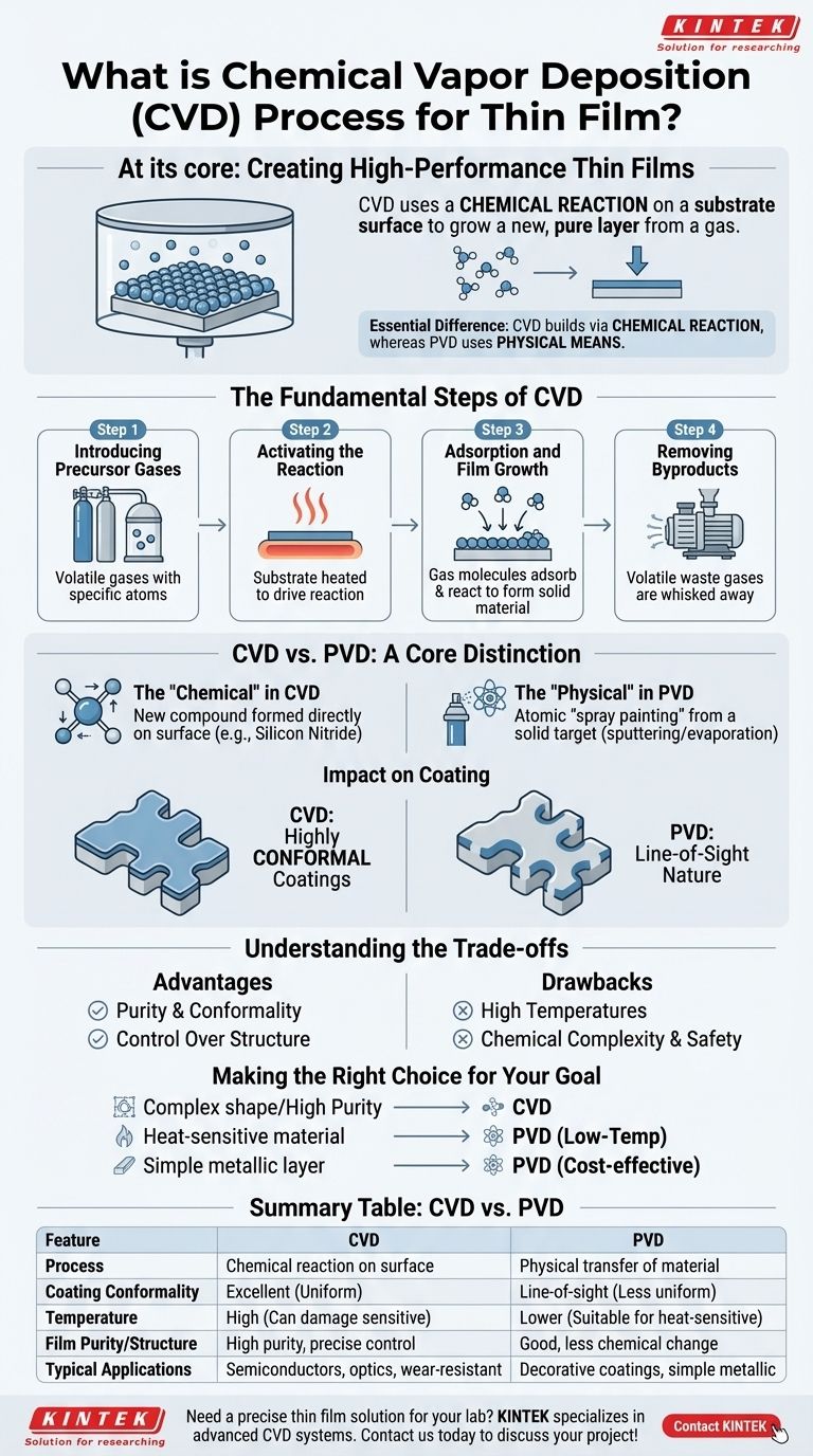
At its core, Chemical Vapor Deposition (CVD) is a process for creating high-performance, solid thin films on a surface from a gas. Unlike physical methods that simply move material, CVD uses a chemical reaction on a substrate's surface to "grow" a new layer. This allows for exceptional control over the film's purity, thickness, and structure, making it a cornerstone technology in manufacturing semiconductors, optics, and advanced coatings.
The essential difference to remember is that CVD builds a film through a chemical reaction on a surface, whereas its counterpart, Physical Vapor Deposition (PVD), uses physical means like evaporation to deposit a film. This distinction is the key to understanding why each method is chosen for different applications.
The Fundamental Steps of CVD
To understand CVD, it's best to visualize it as a precise, atomic-scale construction process that occurs within a controlled chamber.
Step 1: Introducing Precursor Gases
The process begins by introducing volatile precursor gases into a reaction chamber. These gases contain the specific atoms (like silicon, carbon, or titanium) that will ultimately form the final thin film.
Step 2: Activating the Reaction
The substrate—the material to be coated—is heated to a precise temperature. This heat provides the necessary energy to drive the chemical reaction when the precursor gases come into contact with the surface.
Step 3: Adsorption and Film Growth
Gas molecules land and adsorb, or stick, to the hot substrate. The thermal energy at the surface breaks down the precursor molecules, causing a chemical reaction that deposits the desired solid material directly onto the substrate.
Step 4: Removing Byproducts
This chemical reaction also creates volatile byproducts. These are simply waste gases that are whisked away by a vacuum system, leaving behind only the pure, solid thin film. This process repeats, building the film one atomic layer at a time.
CVD vs. PVD: A Core Distinction
While both CVD and PVD create thin films, their underlying principles lead to vastly different capabilities and outcomes.
The "Chemical" in Chemical Vapor Deposition
The defining feature of CVD is the chemical transformation. The material deposited on the substrate is often a new compound formed directly on the surface. This is why CVD is essential for creating materials like silicon nitride or titanium carbide from their constituent gases.
The "Physical" in Physical Vapor Deposition
PVD methods, such as sputtering or evaporation, work like atomic spray painting. A solid source material (the "target") is bombarded with energy, liberating atoms that travel through a vacuum and physically coat the substrate. The material itself does not change its chemical identity during the process.
The Impact on the Final Coating
Because the CVD process is driven by a chemical reaction that occurs everywhere on a heated surface, it produces highly conformal coatings. This means it can uniformly cover complex, three-dimensional shapes, which is a significant advantage over the more "line-of-sight" nature of most PVD processes.
Understanding the Trade-offs
No single deposition method is perfect for every situation. Choosing between CVD and other techniques involves clear trade-offs.
Advantage: Purity and Conformality
CVD can produce exceptionally pure, dense, and uniform films. Its ability to evenly coat intricate geometries is critical in microelectronics, where components have complex topography.
Advantage: Control Over Structure
By carefully controlling temperature, pressure, and gas composition, CVD allows for precise engineering of the film's crystalline structure and properties, such as hardness or electrical conductivity.
Drawback: High Temperatures
A primary limitation of traditional CVD is the high temperature required to drive the reaction. This heat can damage thermally sensitive substrates, such as plastics or electronic devices with pre-existing low-melting-point materials.
Drawback: Chemical Complexity and Safety
The precursor gases used in CVD can be highly toxic, corrosive, or flammable, requiring complex and expensive safety and handling systems. This often makes the process more costly than PVD alternatives.
Making the Right Choice for Your Goal
The ideal deposition method is determined entirely by the desired film properties and the nature of your substrate.
- If your primary focus is a highly pure, uniform coating on a complex shape: CVD is often the superior choice due to its excellent conformality and the quality of the films it produces.
- If your primary focus is coating a heat-sensitive material: A low-temperature PVD process like sputtering is almost always the necessary alternative to avoid damaging the substrate.
- If your primary focus is depositing a simple metallic layer on a flat surface: PVD can often provide a faster, more cost-effective solution without the chemical complexity of CVD.
Ultimately, understanding the fundamental difference between a chemical reaction and a physical transfer is the key to selecting the right tool for your material engineering challenge.
Summary Table:
| Feature | Chemical Vapor Deposition (CVD) | Physical Vapor Deposition (PVD) |
|---|---|---|
| Process | Chemical reaction on substrate surface | Physical transfer of material (e.g., sputtering) |
| Coating Conformality | Excellent (uniform on complex shapes) | Line-of-sight (less uniform on 3D surfaces) |
| Temperature | High (can damage sensitive substrates) | Lower (suitable for heat-sensitive materials) |
| Film Purity/Structure | High purity, precise crystalline control | Good, but less chemical transformation |
| Typical Applications | Semiconductors, optics, wear-resistant coatings | Decorative coatings, simple metallic layers |
Need a precise thin film solution for your lab? KINTEK specializes in lab equipment and consumables, serving laboratory needs with advanced CVD systems that deliver high-purity, conformal coatings for semiconductors, optics, and R&D. Let our experts help you select the right deposition method for your specific substrate and application. Contact us today to discuss your project and enhance your material engineering capabilities!
Visual Guide
Related Products
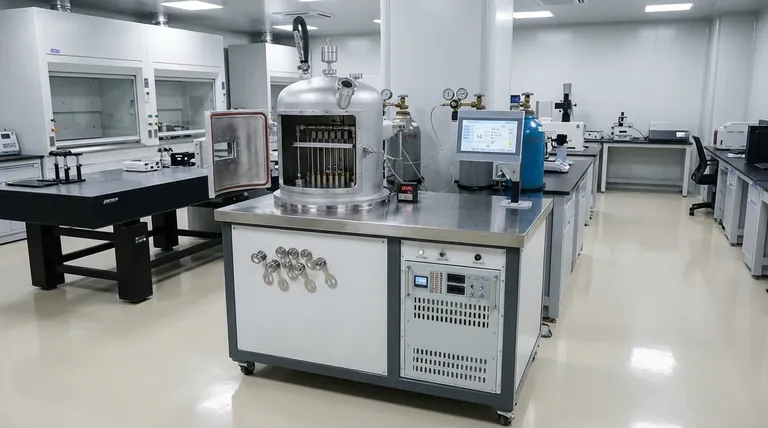
- Chemical Vapor Deposition CVD Equipment System Chamber Slide PECVD Tube Furnace with Liquid Gasifier PECVD Machine
- RF PECVD System Radio Frequency Plasma-Enhanced Chemical Vapor Deposition RF PECVD
- 915MHz MPCVD Diamond Machine Microwave Plasma Chemical Vapor Deposition System Reactor
- Customer Made Versatile CVD Tube Furnace Chemical Vapor Deposition Chamber System Equipment
- Microwave Plasma Chemical Vapor Deposition MPCVD Machine System Reactor for Lab and Diamond Growth
People Also Ask
- What types of substrates are used in CVD to facilitate graphene films? Optimize Graphene Growth with the Right Catalyst
- What are the core advantages of PE-CVD in OLED encapsulation? Protect Sensitive Layers with Low-Temp Film Deposition
- What are the advantages of chemical vapor deposition? Achieve Superior Thin Films for Your Lab
- What is the chemical vapor deposition growth process? Build Superior Thin Films from the Atom Up
- How expensive is chemical vapor deposition? Understanding the True Cost of High-Performance Coating


