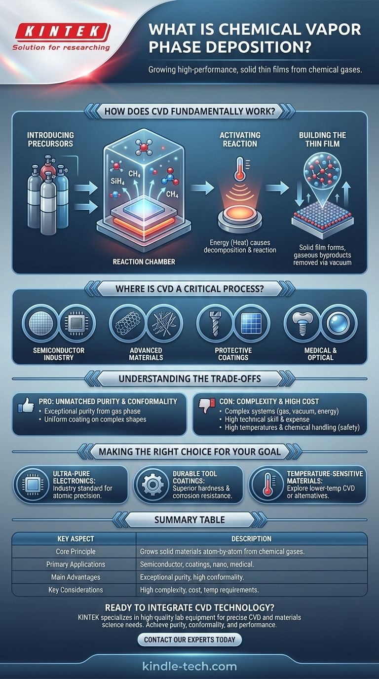
In essence, Chemical Vapor Deposition (CVD) is a highly controlled manufacturing process used to create high-performance, solid thin films on a surface. It works by introducing volatile precursor chemicals in a gas phase into a reaction chamber, where they decompose and react on a heated substrate, building a new material layer by layer.
The core principle of CVD is not merely to coat a surface, but to grow a new solid material directly onto it from chemical gases. This atomic-level control is what makes it a fundamental technology in advanced manufacturing, particularly for electronics and specialized materials.
How Does CVD Fundamentally Work?
The CVD process can be broken down into a sequence of controlled steps, each critical to the quality of the final film. It is a synthesis of chemistry, thermodynamics, and fluid dynamics within a highly specialized environment.
Introducing the Precursors
The process begins by introducing precise amounts of precursor chemicals, which are in a gaseous state, into a reaction chamber. These gases contain the specific elements required to form the final film (e.g., silicon, carbon, nitrogen).
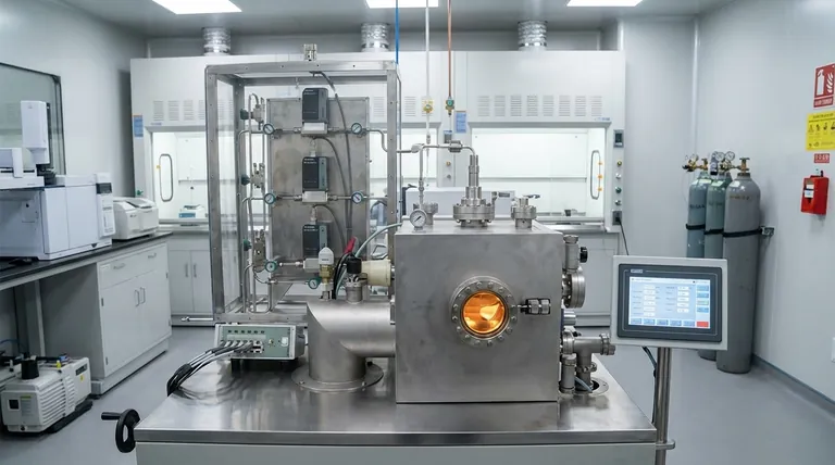
The Reaction Chamber
The workpiece, or substrate, is placed inside a sealed chamber. This chamber is typically put under a vacuum to remove any unwanted contaminants that could interfere with the chemical reaction and compromise the purity of the film.
Activating the Chemical Reaction
An energy source, most commonly heat, is applied to the substrate. This high temperature provides the necessary energy to cause the precursor gases to react with each other or decompose directly on the substrate's surface.
Building the Thin Film
As the chemical reaction occurs, a solid material is deposited onto the substrate, forming a thin, uniform, and tightly bonded film. Gaseous byproducts from the reaction are removed from the chamber by the vacuum and exhaust system, leaving only the desired material behind.
Where is CVD a Critical Process?
CVD's ability to produce extremely pure and uniform films makes it indispensable across several high-technology sectors. The properties of the final product are determined by the specific chemistry and process conditions used.
The Semiconductor Industry
This is the most well-known application. CVD is used to deposit various layers of semiconducting, insulating, and conducting materials onto silicon wafers. This layering process is the foundation for manufacturing integrated circuits and microprocessors.
Advanced Materials and Nanotechnology
CVD is a key method for synthesizing advanced materials with unique properties. It is used to grow structures like carbon nanotubes and GaN nanowires, which have applications in everything from electronics to composites.
Protective and Functional Coatings
The process is used to apply extremely hard and corrosion-resistant coatings on cutting tools, extending their lifespan and improving performance. It is also used to deposit photovoltaic materials onto substrates for the manufacturing of thin-film solar cells.
Medical and Optical Applications
CVD creates biocompatible coatings for medical implants and devices, improving their durability and interaction with the body. It is also used to produce specialized optical coatings and even components for holographic displays.
Understanding the Trade-offs
While powerful, CVD is not a universal solution. Its precision and performance come with significant technical requirements and limitations that must be considered.
Pro: Unmatched Purity and Conformality
Because the film is built from a gas phase, CVD can create materials of exceptionally high purity. Furthermore, it can uniformly coat highly complex and irregular shapes, a feature known as high conformality.
Con: Complexity and High Cost
CVD systems are complex and expensive. They require integrated gas delivery, vacuum, energy, and control systems. Operating these systems effectively requires a high level of technical skill and expertise.
Con: High Temperatures and Chemical Handling
Many traditional CVD processes require very high temperatures, which can damage sensitive substrates like plastics or certain metals. Additionally, the precursor chemicals can be toxic, flammable, or corrosive, demanding stringent safety protocols.
Making the Right Choice for Your Goal
Selecting CVD depends entirely on the material requirements of your application. The decision hinges on whether the superior quality of a CVD film justifies its complexity and cost.
- If your primary focus is creating ultra-pure, high-performance electronic components: CVD is the industry standard due to its atomic-level precision and ability to build complex layered structures.
- If your primary focus is applying a durable, wear-resistant coating on robust tools: CVD provides superior hardness and corrosion resistance that can significantly extend the life of high-value parts.
- If your primary focus is coating temperature-sensitive or low-cost materials: You may need to explore lower-temperature CVD variants or investigate alternative deposition methods entirely.
Ultimately, Chemical Vapor Deposition is the enabling technology for applications where material performance at the microscopic level is non-negotiable.
Summary Table:
| Key Aspect | Description |
|---|---|
| Core Principle | Grows solid materials atom-by-atom from chemical gases onto a substrate. |
| Primary Applications | Semiconductor manufacturing, protective coatings, nanotechnology, medical devices. |
| Main Advantages | Exceptional purity, uniform coating on complex shapes (high conformality). |
| Key Considerations | High process complexity, cost, and often requires high temperatures. |
Ready to Integrate CVD Technology into Your Lab?
Chemical Vapor Deposition is critical for creating the high-performance materials that drive innovation. Whether you are developing next-generation semiconductors, durable tool coatings, or advanced nanomaterials, having the right equipment is essential.
KINTEK specializes in providing high-quality lab equipment and consumables to meet your precise CVD and materials science needs. Our expertise can help you select the ideal system to achieve the purity, conformality, and performance your projects demand.
Contact our experts today to discuss how we can support your research and production goals with reliable, cutting-edge solutions.
Visual Guide
Related Products
- CVD Diamond Dressing Tools for Precision Applications
- Multi Heating Zones CVD Tube Furnace Machine Chemical Vapor Deposition Chamber System Equipment
- CVD Diamond Domes for Industrial and Scientific Applications
- CVD Diamond for Thermal Management Applications
- Chemical Vapor Deposition CVD Equipment System Chamber Slide PECVD Tube Furnace with Liquid Gasifier PECVD Machine
People Also Ask
- What are the disadvantages of CVD diamonds? Understanding the trade-offs for your purchase.
- Can CVD diamonds change color? No, their color is permanent and stable.
- What is chemical vapor deposition of diamond? Grow High-Purity Diamonds Atom-by-Atom
- How do you identify a CVD diamond? The Definitive Guide to Lab-Grown Diamond Verification
- What color diamonds are CVD? Understanding the Process from Brown Tint to Colorless Beauty


