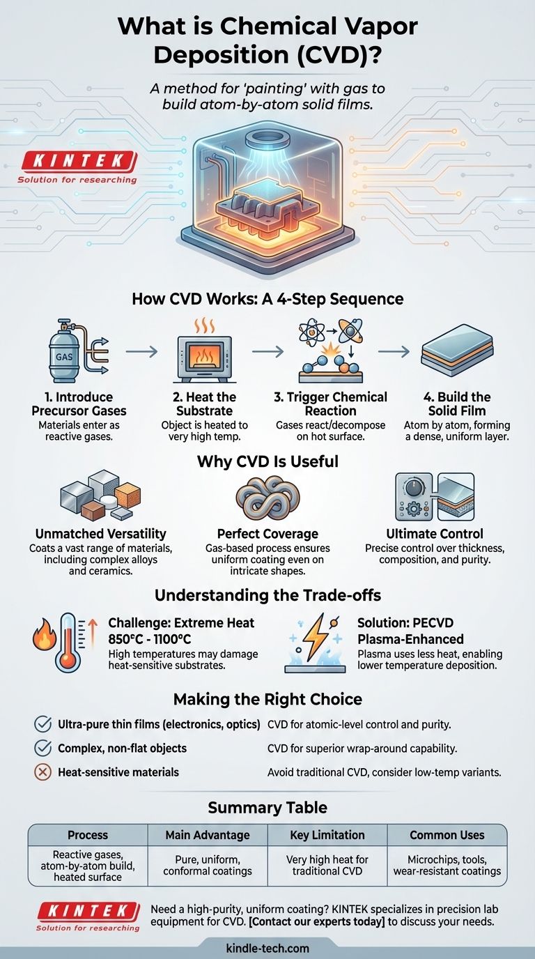
In simple terms, Chemical Vapor Deposition (CVD) is a method for "painting" with gas. Instead of using liquid paint, this process uses reactive gases in a high-temperature chamber to deposit an exceptionally thin and high-quality solid film onto a surface, atom by atom.
Chemical Vapor Deposition is fundamentally a manufacturing technique for building high-performance, ultra-thin solid layers on a surface (the substrate). It achieves this by introducing precursor gases into a chamber, which then react or decompose on the hot substrate to form the desired solid material.
How Does CVD Actually Work?
At its core, the CVD process can be understood as a three-step sequence involving gas, heat, and a chemical reaction. It is a precise and highly controlled method for building materials from the ground up.
Step 1: Introduce Gaseous Ingredients
The materials that will form the final solid film are first introduced into a reaction chamber as gases. These are often called precursor gases.
Step 2: Heat the Surface
The object to be coated, known as the substrate, is placed inside the chamber and heated to a very high temperature. This heat provides the energy needed for the next step to occur.
Step 3: Trigger a Chemical Reaction
When the precursor gases come into contact with the hot substrate, they undergo a chemical reaction or decomposition. This reaction causes the atoms to settle out of the gas and bond to the surface, forming a solid layer.
Step 4: Build the Solid Film
This process continues, building up the solid film one atomic layer at a time. The result is an exceptionally pure, dense, and uniform coating that perfectly conforms to the shape of the substrate.
Why Is CVD So Useful?
CVD is not just one technique but a versatile platform used to create critical components in industries from microelectronics to aerospace. Its advantages stem from the high degree of control it offers.
Unmatched Versatility
CVD can be used to deposit a vast range of materials. This includes metals, non-metals, complex alloys, and advanced ceramic compounds that are prized for their hardness and heat resistance.
Perfect Coverage on Complex Shapes
Because the coating is built from a gas, it can reach and uniformly cover every nook and cranny of a complex, three-dimensional object. This is known as a good wrap-around property, which is very difficult to achieve with liquid-based coating methods.
Ultimate Control and Purity
Technicians can precisely control the final film’s properties—such as its thickness, chemical composition, and crystal structure—by adjusting parameters like temperature, pressure, and gas mixture. This results in films of extremely high purity and density.
Understanding the Trade-offs
While powerful, the traditional CVD process has one significant limitation that determines where and how it can be used.
The Primary Challenge: Extreme Heat
Classic CVD processes require very high temperatures, often between 850°C and 1100°C. This intense heat means that the substrate material itself must be able to withstand it without melting, warping, or degrading.
Modern Solutions
To overcome this heat limitation, specialized versions of the process have been developed. Techniques like Plasma-Enhanced CVD (PECVD) use plasma instead of just heat to energize the gases, allowing deposition to occur at much lower temperatures.
Making the Right Choice for Your Goal
Understanding the core strengths of CVD helps clarify its ideal applications.
- If your primary focus is creating an ultra-pure, flawless thin film for electronics or optics: CVD is the gold standard due to its atomic-level control and high purity.
- If your primary focus is coating a complex, non-flat object with a uniform protective layer: CVD's "wrap-around" capability makes it a superior choice over line-of-sight methods.
- If your primary focus is working with heat-sensitive materials like plastics or certain alloys: You should avoid traditional CVD and instead investigate lower-temperature variants.
Ultimately, Chemical Vapor Deposition empowers engineers to construct materials with a precision that is simply not possible with other methods.
Summary Table:
| Key Aspect | Simple Explanation |
|---|---|
| Process | Using reactive gases to build a solid film atom by atom on a heated surface. |
| Main Advantage | Creates exceptionally pure, uniform, and conformal coatings on complex shapes. |
| Key Limitation | Traditional CVD requires very high temperatures, unsuitable for heat-sensitive materials. |
| Common Uses | Manufacturing microchips, cutting tools, and wear-resistant coatings. |
Need a high-purity, uniform coating for your components?
KINTEK specializes in precision lab equipment and consumables for advanced material deposition processes like CVD. Whether you are developing next-generation electronics, durable tool coatings, or specialized optics, our solutions help you achieve the ultimate control and purity your research demands.
Contact our experts today to discuss how we can support your laboratory's specific coating and thin-film needs.
Visual Guide
Related Products
- Chemical Vapor Deposition CVD Equipment System Chamber Slide PECVD Tube Furnace with Liquid Gasifier PECVD Machine
- RF PECVD System Radio Frequency Plasma-Enhanced Chemical Vapor Deposition RF PECVD
- Microwave Plasma Chemical Vapor Deposition MPCVD Machine System Reactor for Lab and Diamond Growth
- Customer Made Versatile CVD Tube Furnace Chemical Vapor Deposition Chamber System Equipment
- 915MHz MPCVD Diamond Machine Microwave Plasma Chemical Vapor Deposition System Reactor
People Also Ask
- What are the core advantages of PE-CVD in OLED encapsulation? Protect Sensitive Layers with Low-Temp Film Deposition
- What types of substrates are used in CVD to facilitate graphene films? Optimize Graphene Growth with the Right Catalyst
- What are the advantages of chemical vapor deposition? Achieve Superior Thin Films for Your Lab
- Why is Chemical Vapor Deposition (CVD) equipment uniquely suited for constructing hierarchical superhydrophobic structures?
- What are the processes of vapor phase deposition? Understand CVD vs. PVD for Superior Thin Films


