At its core, Chemical Vapor Deposition (CVD) is a highly controlled manufacturing process used to create high-purity, high-performance solid materials, typically as thin films. In electronics, this process is not just an ancillary step; it is a fundamental technique for fabricating the advanced conductors, insulators, and semiconductors that form the building blocks of virtually all modern devices.
CVD is the foundational process that allows engineers to "grow" specialized materials with atomic-level precision. By converting gaseous chemicals into solid layers on a substrate, it enables the creation of components with the exact electrical, thermal, or optical properties required for high-performance electronics.
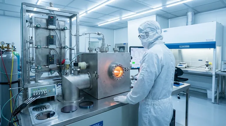
How Chemical Vapor Deposition Works
CVD is a sophisticated method for depositing a material from a gaseous state onto a solid surface, known as a substrate. The entire process takes place within a controlled vacuum chamber.
The Basic Principle: From Gas to Solid
The process begins by introducing one or more volatile precursor gases into the chamber. These gases contain the chemical elements that will make up the final film.
For example, to create a silicon film, a precursor gas like silane (SiH₄) might be used.
The Role of the Substrate
Inside the chamber is a substrate, which is the material upon which the new film will be grown. In electronics, this is most often a silicon wafer or another semiconductor material.
The substrate is heated to a specific, high temperature, which provides the energy needed to drive the chemical reaction.
The Chemical Reaction and Deposition
When the precursor gases come into contact with the heated substrate, they undergo a chemical reaction and decompose.
The desired solid material from this reaction deposits onto the substrate, forming a thin, uniform film. Other gaseous byproducts are removed from the chamber by the vacuum system.
Why CVD is Essential for Electronics
The ability to create extremely pure and uniform thin films is what makes CVD indispensable. These films can be engineered to have very specific properties, making them critical for different functions within an electronic device.
Fabricating Conductors and Insulators
CVD is used to deposit a wide range of materials. Some, like CVD graphene, are prized for their superior electrical conductivity and are used in advanced displays and superconductors.
Others, like silicon dioxide, are excellent electrical insulators, essential for building the gate structures in transistors that control the flow of current.
Creating High-Performance Structures
Beyond simple layers, CVD is used to build complex structures. It can create diffusion barriers, which are ultra-thin films that prevent different materials within a chip from mixing and degrading performance.
It's also used to grow materials with exceptional thermal properties. For instance, synthetic diamond films, grown via CVD, are used as high-conductivity heat sinks to draw damaging heat away from power electronics.
Understanding the Trade-offs
While powerful, CVD is a complex process with specific requirements and is not the only deposition method available. Understanding its context is key.
CVD vs. PVD: A Key Distinction
CVD is often compared to Physical Vapor Deposition (PVD). The primary difference is how the material is delivered to the substrate.
CVD uses a chemical reaction to transform a gas into a solid film. In contrast, PVD uses physical means—such as evaporation or sputtering—to transport a solid material through a vapor phase and onto the substrate without a chemical change.
Process Complexity and Control
The quality of a CVD film depends on precise control over temperature, pressure, gas flow rates, and chemistry. This makes the equipment sophisticated and the process itself sensitive.
Maintaining this control is necessary to achieve the uniformity and purity required for high-yield semiconductor manufacturing.
Making the Right Choice for Your Goal
Applying CVD is about leveraging its unique capabilities to solve a specific engineering challenge. The material you create is determined entirely by the goal you need to achieve.
- If your primary focus is advanced semiconductor processing: You will use CVD to create the atomically thin and pure insulating and conducting films required for modern logic and memory chips.
- If your primary focus is thermal management: You will leverage CVD to grow synthetic diamond or other high-conductivity films to act as efficient heat spreaders for high-power devices.
- If your primary focus is next-generation displays or sensors: You will employ CVD to produce large-area, transparent, and conductive graphene films.
Ultimately, Chemical Vapor Deposition is the cornerstone technology that enables material innovation at the atomic scale, making our most advanced electronics possible.
Summary Table:
| CVD Application | Key Material Examples | Primary Function in Electronics |
|---|---|---|
| Semiconductor Processing | Silicon, Silicon Dioxide | Create insulating & conducting layers for logic/memory chips |
| Thermal Management | Synthetic Diamond | Act as high-conductivity heat spreaders for power devices |
| Advanced Displays/Sensors | Graphene | Produce large-area, transparent conductive films |
Ready to integrate high-purity thin films into your electronic devices? KINTEK specializes in providing advanced lab equipment and consumables for precise Chemical Vapor Deposition processes. Whether you're developing next-generation semiconductors, improving thermal management, or creating innovative displays, our solutions help you achieve atomic-level precision and superior material performance. Contact our experts today to discuss how we can support your laboratory's specific CVD needs!
Visual Guide

Related Products
- CVD Diamond Dressing Tools for Precision Applications
- Multi Heating Zones CVD Tube Furnace Machine Chemical Vapor Deposition Chamber System Equipment
- CVD Diamond Domes for Industrial and Scientific Applications
- CVD Diamond for Thermal Management Applications
- Chemical Vapor Deposition CVD Equipment System Chamber Slide PECVD Tube Furnace with Liquid Gasifier PECVD Machine
People Also Ask
- How do CVD diamonds grow? A Step-by-Step Guide to Lab-Grown Diamond Creation
- Can CVD diamonds change color? No, their color is permanent and stable.
- What color diamonds are CVD? Understanding the Process from Brown Tint to Colorless Beauty
- Does the chemical vapor deposition be used for diamonds? Yes, for Growing High-Purity Lab Diamonds
- What are the disadvantages of CVD diamonds? Understanding the trade-offs for your purchase.


