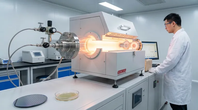
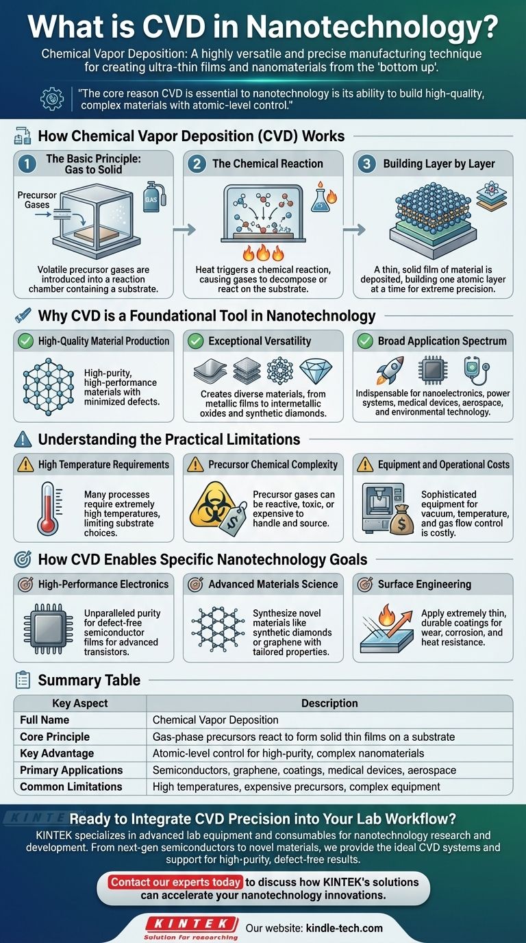
In nanotechnology, CVD stands for Chemical Vapor Deposition. It is a highly versatile and precise manufacturing technique used to create ultra-thin films and nanomaterials. The process involves introducing precursor gases into a chamber where they react and deposit a solid material, layer by layer, onto a substrate.
The core reason CVD is essential to nanotechnology is its ability to build high-quality, complex materials from the "bottom up." This atomic-level control is critical for fabricating the innovative structures required for next-generation electronics, medicine, and energy.
How Chemical Vapor Deposition (CVD) Works
CVD is fundamentally a process of transformation, turning gas molecules into a solid, highly-ordered film. It’s analogous to how frost forms on a window, but in a highly controlled, high-temperature environment.
The Basic Principle: Gas to Solid
The process begins by introducing one or more volatile precursor gases into a reaction chamber that contains a base material, known as a substrate.
The Chemical Reaction
The chamber is heated to a specific temperature, providing the energy needed to trigger a chemical reaction. This causes the precursor gases to decompose or react with each other on the surface of the substrate.
Building Layer by Layer
As the reaction occurs, a thin, solid film of the desired material is deposited onto the substrate. This process is continued, building up the material one atomic layer at a time, which allows for extreme precision in thickness and material properties.
Why CVD is a Foundational Tool in Nanotechnology
While other deposition techniques exist, CVD is one of the most widely employed for synthesizing nanomaterials because of its unique advantages.
High-Quality Material Production
CVD is renowned for producing high-purity, high-performance materials. The controlled nature of the process minimizes defects, which is critical for applications like semiconductors and nanoelectronics.
Exceptional Versatility
The technique is not limited to one type of material. It can be used to create everything from simple metallic films to complex, multi-component structures, intermetallic oxides, and even synthetic diamonds.
Broad Application Spectrum
This versatility makes CVD indispensable across many advanced industries. It is used to develop components for nanoelectronics, power systems, medical devices, aerospace engineering, and environmental technology.
Understanding the Practical Limitations
Despite its power, CVD is not a universal solution. Understanding its trade-offs is key to its successful application.
High Temperature Requirements
Many CVD processes require extremely high temperatures to initiate the necessary chemical reactions. This can limit the types of substrate materials that can be used, as some may not withstand the heat.
Precursor Chemical Complexity
The process relies on precursor gases that are often highly reactive, toxic, or expensive. Safely handling and sourcing these chemicals adds complexity and cost to the manufacturing process.
Equipment and Operational Costs
Achieving the necessary vacuum, temperature control, and gas flow precision requires sophisticated and expensive equipment. This can make the initial investment and operational costs significant.
How CVD Enables Specific Nanotechnology Goals
The right manufacturing process depends entirely on your end goal. Here is how to think about applying CVD.
- If your primary focus is high-performance electronics: CVD provides the unparalleled purity and uniformity needed to create defect-free semiconductor films for advanced transistors.
- If your primary focus is advanced materials science: This technique is a powerful tool for synthesizing novel materials, such as synthetic diamonds or graphene, with precisely tailored properties.
- If your primary focus is surface engineering: CVD allows you to apply extremely thin, durable, and functional coatings to a surface, enhancing its resistance to wear, corrosion, or heat.
Ultimately, Chemical Vapor Deposition gives engineers and scientists the atomic-level control needed to build the foundational materials of modern technology.
Summary Table:
| Key Aspect | Description |
|---|---|
| Full Name | Chemical Vapor Deposition |
| Core Principle | Gas-phase precursors react to form solid thin films on a substrate |
| Key Advantage | Atomic-level control for high-purity, complex nanomaterials |
| Primary Applications | Semiconductors, graphene, coatings, medical devices, aerospace |
| Common Limitations | High temperatures, expensive precursors, complex equipment |
Ready to Integrate CVD Precision into Your Lab Workflow?
KINTEK specializes in providing advanced lab equipment and consumables for nanotechnology research and development. Whether you are developing next-generation semiconductors, synthesizing novel materials like graphene, or applying functional coatings, having the right tools is critical.
Our expertise can help you select the ideal CVD system or support consumables for your specific application, ensuring you achieve the high-purity, defect-free results your projects demand.
Contact our experts today to discuss how KINTEK's solutions can accelerate your nanotechnology innovations.
Visual Guide
Related Products
- CVD Diamond Dressing Tools for Precision Applications
- Multi Heating Zones CVD Tube Furnace Machine Chemical Vapor Deposition Chamber System Equipment
- CVD Diamond Domes for Industrial and Scientific Applications
- CVD Diamond for Thermal Management Applications
- Chemical Vapor Deposition CVD Equipment System Chamber Slide PECVD Tube Furnace with Liquid Gasifier PECVD Machine
People Also Ask
- What are the raw materials for CVD diamonds? A seed, a gas, and the science of crystal growth.
- Can CVD diamonds change color? No, their color is permanent and stable.
- How do CVD diamonds grow? A Step-by-Step Guide to Lab-Grown Diamond Creation
- How long does it take to make synthetic diamonds? Discover the 6-8 Week Science Behind Lab-Grown Gems
- How do you identify a CVD diamond? The Definitive Guide to Lab-Grown Diamond Verification


