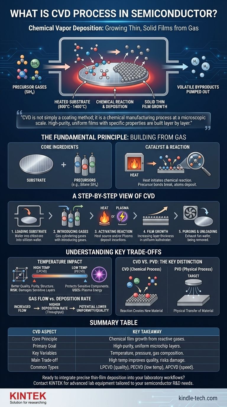
At its core, Chemical Vapor Deposition (CVD) is a highly controlled process used to "grow" thin, solid films of material onto a surface from a gas. In semiconductor manufacturing, this process is fundamental for building the intricate, layered structures of a microchip. It works by introducing specific precursor gases into a reaction chamber where they chemically react at the surface of a heated substrate (like a silicon wafer), depositing the desired material layer by layer.
The crucial insight is that CVD is not simply a coating method; it is a chemical manufacturing process at a microscopic scale. By precisely controlling variables like temperature, pressure, and gas composition, engineers can build high-purity, uniform films with specific properties, forming the essential insulating, conducting, and semiconducting layers of an integrated circuit.

The Fundamental Principle: Building from Gas
To truly understand CVD, it's best to think of it as a form of molecular or atomic construction. Instead of carving material away, you are adding it with extreme precision.
The Core Ingredients: Substrate and Precursors
The process requires two primary components. The first is the substrate, which is the foundational material being coated, typically a silicon wafer in semiconductor fabrication.
The second is a set of precursor gases. These are volatile chemical compounds that contain the specific atoms needed for the final film. For example, to deposit a film of pure silicon, a gas like silane (SiH₄) might be used.
The Catalyst: The Role of Heat
Heat provides the energy needed to initiate the chemical reaction. The substrate is heated to a precise temperature, often between 800°C and 1400°C.
When the precursor gases flow over this hot surface, the thermal energy breaks their chemical bonds. This allows the desired atoms (like silicon) to be released and bond to the substrate surface.
The Reaction and Deposition
The chemical reactions occur directly on or very near the heated substrate. As the reaction proceeds, a solid film grows uniformly across the surface.
Any unreacted precursor gas and chemical byproducts are volatile and are continuously pumped out of the chamber as waste. The result is a stable, solid thin film permanently bonded to the substrate.
A Step-by-Step View of the CVD Process
While there are many variations, the core sequence of a CVD process remains consistent.
1. Loading the Substrate
Wafers are carefully placed inside a sealed, controlled process chamber.
2. Introducing the Gases
A precise mixture of precursor gases and carrier gases (inert gases like nitrogen or argon) is introduced into the chamber at a controlled flow rate.
3. Activating the Reaction
The chamber and substrate are brought to the target temperature. In some advanced CVD methods, an energy source like an RF plasma is also used to help break down the gas molecules at lower temperatures.
4. Film Growth
The chemical reaction proceeds, and the film grows on the wafer surface. This stage is carefully timed to achieve the exact thickness required for the device being built.
5. Purging and Unloading
The flow of reactive gases is stopped, the chamber is purged with inert gas, and the newly coated wafers are removed.
Understanding the Key Trade-offs
The power of CVD lies in its tunability, but this also introduces critical trade-offs that engineers must manage.
The Impact of Temperature
Temperature is the most critical variable. High temperatures generally produce films with higher purity and better crystalline structure. However, they can also damage previously fabricated layers on the chip.
This is why different types of CVD exist. Low-Pressure CVD (LPCVD) uses high heat for excellent film quality, while Plasma-Enhanced CVD (PECVD) uses an energy-rich plasma to enable reactions at much lower temperatures, protecting sensitive components.
Gas Flow vs. Deposition Rate
The rate at which the film grows is directly related to the concentration and flow rate of the precursor gases. Increasing the flow can speed up the process (increasing throughput), but it can also negatively impact the uniformity and quality of the film.
CVD vs. PVD: The Key Distinction
CVD is often compared to Physical Vapor Deposition (PVD). The essential difference is simple:
- CVD is a chemical process. The precursor gases are chemically different from the final solid film. A reaction creates a new material on the substrate.
- PVD is a physical process. A solid source material is physically transferred (by evaporation or sputtering) onto the substrate without a chemical reaction.
Making the Right Choice for Your Goal
The specific CVD technique used is always dictated by the requirements of the layer being deposited.
- If your primary focus is creating a high-purity, perfectly ordered crystalline layer (e.g., epitaxy): You will use a high-temperature CVD process like LPCVD to ensure the best possible film quality.
- If your primary focus is depositing an insulating film over existing metal circuitry: You must use a low-temperature PECVD process to prevent the metal from melting or being damaged.
- If your primary focus is achieving high throughput for non-critical, thicker films: A process like Atmospheric Pressure CVD (APCVD) might be chosen for its high deposition speed.
Ultimately, Chemical Vapor Deposition is a cornerstone technology, enabling the construction of the complex, three-dimensional structures that define every modern electronic device.
Summary Table:
| CVD Aspect | Key Takeaway |
|---|---|
| Core Principle | A chemical process that grows thin films from reactive gases onto a heated substrate. |
| Primary Goal | To build high-purity, uniform insulating, conducting, and semiconducting layers for microchips. |
| Key Variables | Temperature, pressure, and gas composition. |
| Main Trade-off | Higher temperature improves film quality but can damage sensitive chip layers. |
| Common Types | LPCVD (high quality), PECVD (low temperature), APCVD (high speed). |
Ready to integrate precise thin-film deposition into your laboratory workflows? The right CVD equipment is critical for achieving high-purity, uniform layers in semiconductor R&D and production. KINTEK specializes in providing advanced lab equipment and consumables tailored to your specific research and manufacturing challenges. Our experts can help you select the ideal system to enhance your process efficiency and material quality. Contact our team today to discuss your project requirements and discover the KINTEK difference.
Visual Guide
Related Products
- CVD Diamond Dressing Tools for Precision Applications
- Multi Heating Zones CVD Tube Furnace Machine Chemical Vapor Deposition Chamber System Equipment
- CVD Diamond Domes for Industrial and Scientific Applications
- CVD Diamond for Thermal Management Applications
- Chemical Vapor Deposition CVD Equipment System Chamber Slide PECVD Tube Furnace with Liquid Gasifier PECVD Machine
People Also Ask
- What are the disadvantages of CVD diamonds? Understanding the trade-offs for your purchase.
- Can CVD diamonds change color? No, their color is permanent and stable.
- What is CVD diamond? The Ultimate Guide to Lab-Grown Diamonds and Their Uses
- How do you identify a CVD diamond? The Definitive Guide to Lab-Grown Diamond Verification
- How do CVD diamonds grow? A Step-by-Step Guide to Lab-Grown Diamond Creation


