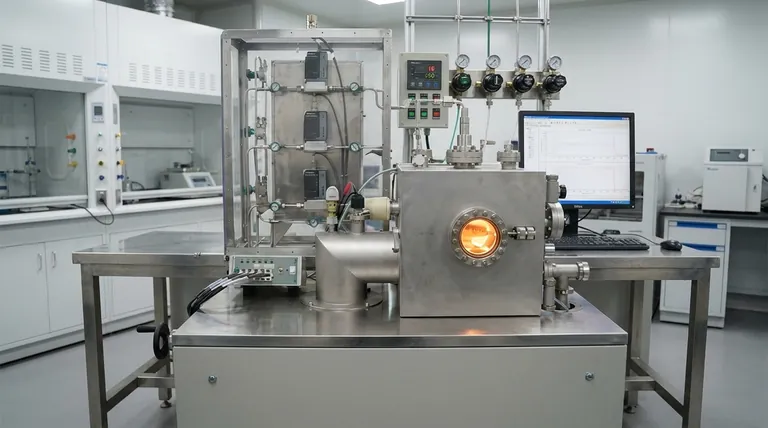
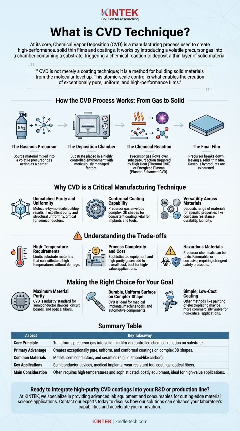
At its core, Chemical Vapor Deposition (CVD) is a manufacturing process used to create high-performance, solid thin films and coatings. It works by introducing a volatile precursor gas into a chamber containing a substrate (the object to be coated). A chemical reaction is triggered on the substrate's surface, causing a thin layer of solid material to deposit, or "grow," onto it, while gaseous byproducts are removed.
Chemical Vapor Deposition is not merely a coating technique; it is a method for building solid materials from the molecular level up. This atomic-scale control is what enables the creation of exceptionally pure, uniform, and high-performance films essential for advanced technology.
How the CVD Process Works: From Gas to Solid
Understanding CVD is to understand a carefully controlled chemical reaction that transforms a gas into a precise solid layer. The process can be broken down into a few key stages.
The Gaseous Precursor
The process begins with the source material mixed into a volatile precursor gas. This gas acts as a carrier, allowing the desired material to be transported efficiently into a reaction chamber.
The Deposition Chamber
Inside the chamber, the object to be coated, known as the substrate, is placed in a highly controlled environment. Factors like temperature, pressure, and gas flow are meticulously managed.
The Chemical Reaction
The precursor gas flows over the substrate, where a reaction is induced. This can be triggered by high heat (Thermal CVD) or an energized plasma (Plasma-Enhanced CVD), causing the precursor to decompose.
The Final Film
As the precursor breaks down, it leaves a solid, thin film of the source material adhered to the substrate's surface. The remaining gaseous byproducts are then exhausted from the chamber, leaving behind an exceptionally pure and uniform layer.
Why CVD is a Critical Manufacturing Technique
CVD is valued in advanced manufacturing because its outputs possess qualities that are difficult to achieve with other methods. Its utility comes from a few core advantages.
Unmatched Purity and Uniformity
Because the film is built up molecule by molecule from a pure gas source, the resulting layer has excellent purity and structural uniformity. This is critical for applications like semiconductors, where even microscopic imperfections can cause device failure.
Conformal Coating Capability
CVD is not a line-of-sight process like spraying. The precursor gas can envelop complex, three-dimensional shapes, ensuring a consistent and even coating on all exposed surfaces. This is vital for parts like medical implants and machine tools.
Versatility Across Materials
The technique is remarkably versatile. It can be used to deposit a wide range of materials, including metals, semiconductors, and ceramics, enabling the creation of materials with specific properties like corrosion resistance, durability, or lubricity.
Understanding the Trade-offs
While powerful, CVD is not a universal solution. Its precision and quality come with specific operational considerations.
High-Temperature Requirements
Many traditional CVD processes require very high temperatures to trigger the chemical reaction. This can limit the types of substrate materials that can be used without being damaged or warped by the heat.
Process Complexity and Cost
CVD equipment is sophisticated and can be expensive to acquire and operate. Furthermore, the high-purity precursor gases required for the process add to the overall cost, making it best suited for high-value applications.
Hazardous Materials
The precursor chemicals used in CVD can be toxic, flammable, or corrosive. This necessitates stringent safety protocols and specialized handling infrastructure, which contributes to the complexity and cost of the operation.
Making the Right Choice for Your Goal
Selecting CVD depends entirely on whether its unique strengths align with your final objective.
- If your primary focus is maximum material purity for electronic or optical performance: CVD is the industry standard for fabricating semiconductor devices, circuit boards, and optical fibers.
- If your primary focus is creating a durable, protective, and uniform surface on a complex shape: CVD is ideal for coating medical implants, machine tools, and automotive components for wear and corrosion resistance.
- If your primary focus is producing a simple, low-cost coating for a non-critical application: Other methods, such as painting or electroplating, may be more commercially viable than the high-precision CVD process.
Ultimately, CVD provides a powerful method for constructing materials from the atom up, enabling the creation of components that would otherwise be impossible to fabricate.
Summary Table:
| Aspect | Key Takeaway |
|---|---|
| Core Principle | Transforms a precursor gas into a solid thin film via a controlled chemical reaction on a substrate surface. |
| Primary Advantage | Creates exceptionally pure, uniform, and conformal coatings on complex 3D shapes. |
| Common Materials | Metals, semiconductors (e.g., silicon), and ceramics (e.g., diamond-like carbon). |
| Key Applications | Semiconductor devices, medical implants, wear-resistant tool coatings, optical fibers. |
| Main Consideration | Often requires high temperatures and sophisticated, costly equipment, making it ideal for high-value applications. |
Ready to integrate high-purity CVD coatings into your R&D or production line?
At KINTEK, we specialize in providing advanced lab equipment and consumables for cutting-edge material science applications. Whether you are developing next-generation semiconductors or need durable coatings for medical devices, our expertise can help you achieve the material purity and performance your projects demand.
Contact our experts today to discuss how our solutions can enhance your laboratory's capabilities and accelerate your innovation.
Visual Guide
Related Products
- Chemical Vapor Deposition CVD Equipment System Chamber Slide PECVD Tube Furnace with Liquid Gasifier PECVD Machine
- HFCVD Machine System Equipment for Drawing Die Nano-Diamond Coating
- Multi Heating Zones CVD Tube Furnace Machine Chemical Vapor Deposition Chamber System Equipment
- CVD Diamond Dressing Tools for Precision Applications
- CVD Diamond Domes for Industrial and Scientific Applications
People Also Ask
- What is the chemical vapor deposition growth process? Build Superior Thin Films from the Atom Up
- What types of substrates are used in CVD to facilitate graphene films? Optimize Graphene Growth with the Right Catalyst
- Why is Chemical Vapor Deposition (CVD) equipment uniquely suited for constructing hierarchical superhydrophobic structures?
- What is plasma enhanced chemical vapor deposition PECVD equipment? A Guide to Low-Temperature Thin Film Deposition
- What are the advantages of chemical vapor deposition? Achieve Superior Thin Films for Your Lab


