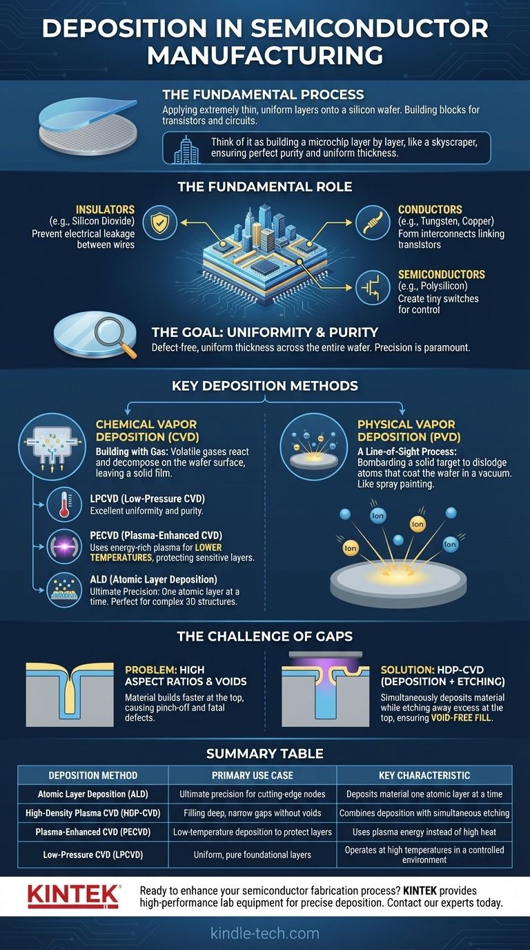
In semiconductor manufacturing, deposition is the fundamental process of applying extremely thin, uniform layers of material onto a silicon wafer. These layers, which can be insulators, conductors, or semiconductors, are the essential building blocks that form the transistors, wires, and other components of an integrated circuit. A variety of highly specialized techniques are used to deposit these films, with the choice of method depending on the specific material and its structural role within the chip.
At its core, deposition is about constructing a microchip layer by layer, much like building a skyscraper floor by floor. The challenge is not just adding a layer, but ensuring it is perfectly pure, uniformly thick, and can flawlessly fill the incredibly complex, microscopic topography of modern processors.
The Fundamental Role of Deposition
Deposition is not a single action but a critical phase of fabrication where the very substance of a circuit is created. Without it, a silicon wafer would remain a blank slate.
Building the Layers of a Microchip
Think of a completed microprocessor as a dense, three-dimensional city with billions of structures. Deposition is the process that builds every component of that city—the foundations, the walls, the electrical wiring, and the insulation between them. Each layer is just nanometers thick and must be near-perfect.
Insulators, Conductors, and Semiconductors
Deposition techniques are used to apply all three primary types of materials needed for a circuit.
- Insulators like silicon dioxide are deposited to prevent electrical current from leaking between wires.
- Conductors like tungsten or copper are deposited to form the "wires" and interconnects that link transistors together.
- Semiconductors like polysilicon are deposited to create the transistor gates themselves—the tiny switches that control the flow of electricity.
The Goal: Uniformity and Purity
The primary goal of any deposition process is to create a defect-free film with uniform thickness across the entire surface of the wafer. Even a microscopic variation, impurity, or void can cause a chip to fail, making the precision of these processes paramount to manufacturing yield.
Key Deposition Methods and Their Purpose
The term "deposition" encompasses a wide family of technologies, each optimized for different materials, temperatures, and structural requirements. They are broadly categorized into two families: Chemical Vapor Deposition (CVD) and Physical Vapor Deposition (PVD).
Chemical Vapor Deposition (CVD): Building with Gas
CVD is the most common family of techniques. In this process, the wafer is placed in a reaction chamber and exposed to one or more volatile gases. These gases react and decompose on the wafer's surface, leaving behind a solid, high-purity film.
Common CVD Variations
Different types of CVD are used to solve different problems, primarily related to temperature and film quality.
- LPCVD (Low-Pressure CVD): This method uses high temperatures and low pressure. The high heat provides the energy for the chemical reaction, resulting in films with excellent uniformity and purity.
- PECVD (Plasma-Enhanced CVD): This method uses an energy-rich plasma to assist the chemical reaction. This added energy means the process can run at much lower temperatures, which is critical when depositing layers on top of materials (like aluminum) that cannot withstand high heat.
Atomic Layer Deposition (ALD): The Ultimate in Precision
For the most advanced and smallest chip features, Atomic Layer Deposition (ALD) is used. This technique deposits material literally one single atomic layer at a time by introducing gases in a sequential, self-limiting cycle. This provides unparalleled control over film thickness and the ability to perfectly coat the most complex 3D structures.
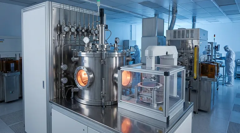
Physical Vapor Deposition (PVD): A Line-of-Sight Process
In contrast to CVD, PVD is a physical process. It involves bombarding a solid "target" of the desired material with high-energy ions, which physically dislodges atoms from the target. These atoms then travel through a vacuum and coat the wafer. It is often described as a "line-of-sight" process, similar to spray painting.
Understanding the Trade-offs: The Challenge of Gaps
As transistors shrink, the trenches and gaps that must be filled with material become extremely deep and narrow. This creates a significant challenge that has driven the evolution of deposition technology.
The Problem of High "Aspect Ratios"
Aspect ratio refers to the ratio of a feature's height to its width. In modern chips, these ratios are very high. When trying to fill a deep, narrow trench with a conventional deposition process, a critical problem emerges.
Voids and "Pinch-Off"
A standard deposition process tends to build up material faster on the top corners of a trench than at the bottom. This can cause the opening to "pinch off" before the trench is completely filled, trapping a hollow space, or void, within the structure. This void is a fatal defect that can ruin the entire chip.
The HDP-CVD Solution: Deposition Plus Etching
To solve this, a more advanced process called High-Density Plasma CVD (HDP-CVD) was developed. This technique cleverly combines two processes in the same chamber:
- Deposition: Material is deposited into the trench.
- Etching: Simultaneously, ions (like argon) are used to physically sputter away, or etch, the material that builds up at the top opening of the trench.
This simultaneous etching action keeps the trench open long enough for the deposition materials to completely fill the feature from the bottom up, ensuring a void-free fill even in the highest aspect ratio structures.
Making the Right Choice for Your Goal
Selecting a deposition method is a matter of balancing the specific requirements of the layer being built—its material, its structure, and the temperature tolerance of the layers already beneath it.
- If your primary focus is ultimate precision and conformity for cutting-edge nodes: Atomic Layer Deposition (ALD) is the standard due to its one-atom-at-a-time control.
- If your primary focus is filling deep, narrow gaps without voids: High-Density Plasma CVD (HDP-CVD) is the solution, as it combines deposition with etching to ensure a complete fill.
- If your primary focus is depositing a film at a lower temperature to protect existing layers: Plasma-Enhanced CVD (PECVD) is the ideal choice, as plasma provides the reaction energy instead of high heat.
- If your primary focus is a uniform, pure foundational layer where high temperature is not a constraint: Low-Pressure CVD (LPCVD) provides excellent results in a highly controlled environment.
Understanding the purpose behind each deposition technique is the first step toward mastering the complexities of modern semiconductor fabrication.
Summary Table:
| Deposition Method | Primary Use Case | Key Characteristic |
|---|---|---|
| Atomic Layer Deposition (ALD) | Ultimate precision for cutting-edge nodes | Deposits material one atomic layer at a time |
| High-Density Plasma CVD (HDP-CVD) | Filling deep, narrow gaps without voids | Combines deposition with simultaneous etching |
| Plasma-Enhanced CVD (PECVD) | Low-temperature deposition to protect layers | Uses plasma energy instead of high heat |
| Low-Pressure CVD (LPCVD) | Uniform, pure foundational layers | Operates at high temperatures in a controlled environment |
Ready to enhance your semiconductor fabrication process?
KINTEK specializes in providing high-performance lab equipment and consumables for precise deposition and other critical semiconductor manufacturing steps. Our solutions help you achieve the uniform, defect-free layers essential for high-yield chip production.
Contact our experts today to discuss how we can support your laboratory's specific deposition needs and drive your innovation forward.
Visual Guide
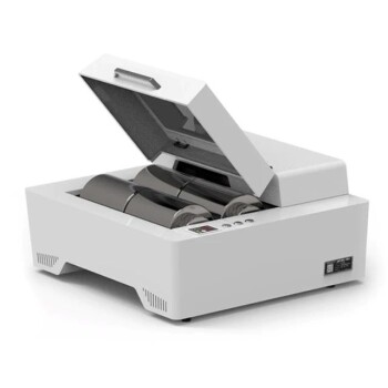
Related Products
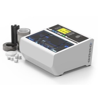
- Chemical Vapor Deposition CVD Equipment System Chamber Slide PECVD Tube Furnace with Liquid Gasifier PECVD Machine
- CVD Diamond Dressing Tools for Precision Applications
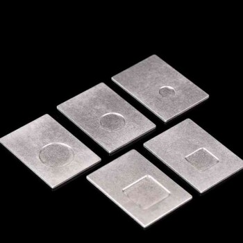
- Molybdenum Tungsten Tantalum Evaporation Boat for High Temperature Applications
- Evaporation Boat for Organic Matter
- Electron Beam Evaporation Coating Oxygen-Free Copper Crucible and Evaporation Boat
People Also Ask
- What happens during deposition chemistry? Building Thin Films from Gaseous Precursors
- How are carbon nanotubes grown? Master Scalable Production with Chemical Vapor Deposition
- How expensive is chemical vapor deposition? Understanding the True Cost of High-Performance Coating
- Why is Chemical Vapor Deposition (CVD) equipment uniquely suited for constructing hierarchical superhydrophobic structures?
- What are the processes of vapor phase deposition? Understand CVD vs. PVD for Superior Thin Films