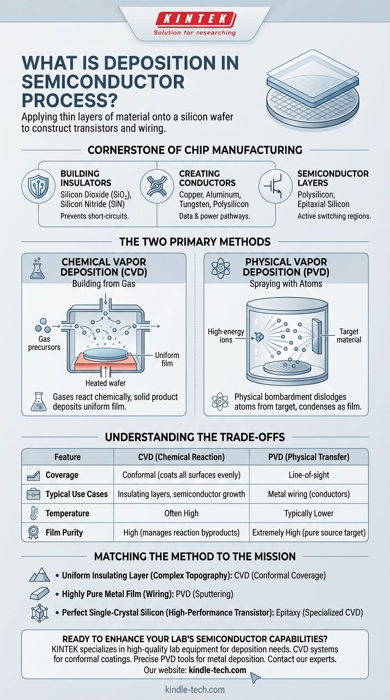
In short, deposition is the process of applying thin layers of material onto a silicon wafer. These carefully controlled films, often just a few atoms thick, are the fundamental building blocks used to construct the intricate, three-dimensional structures that form transistors and the wiring that connects them.
The core purpose of deposition is not simply to add layers, but to precisely build the essential components of an integrated circuit—the conductors, insulators, and semiconductors—that allow it to function.
Why Deposition is a Cornerstone of Chip Manufacturing
Every microchip is a complex city of billions of microscopic components. Deposition is the construction process that builds the structures of this city, layer by painstaking layer.
Building the Insulators
Insulating films, often made of materials like silicon dioxide (SiO₂) or silicon nitride (SiN), are critical. They act as barriers that prevent electrical current from leaking or "short-circuiting" between different conductive paths.
Creating the Conductors
Conductive films form the "wires" and "gates" of the chip. Materials like copper, aluminum, tungsten, and polysilicon are deposited to create the pathways that allow electricity to flow, transmitting data and power throughout the circuit.
Laying Down Semiconductor Layers
Specialized deposition processes are used to grow or place layers of semiconductor material, like polysilicon or epitaxial silicon. These are the "active" regions where the switching action of the transistor takes place.
The Two Primary Methods of Deposition
While there are many specialized techniques, virtually all deposition falls into two major categories: Chemical Vapor Deposition (CVD) and Physical Vapor Deposition (PVD). The choice between them depends entirely on the material being deposited and the structure being built.
Chemical Vapor Deposition (CVD): Building from Gas
CVD is the most common method. It involves introducing one or more gases (precursors) into a reaction chamber containing the wafer.
These gases react chemically, and the solid product of that reaction "deposits" onto the wafer's surface, forming a uniform film. Think of it as precisely controlled frost forming from a chemical reaction in the air.
Physical Vapor Deposition (PVD): Spraying with Atoms
PVD is a physical process, not a chemical one. It works by bombarding a solid source material (a "target") with high-energy ions inside a vacuum.
This bombardment dislodges atoms from the target, which then travel and condense onto the cooler wafer, forming a thin film. This is analogous to an atomic-level spray painting process.
Understanding the Trade-offs: CVD vs. PVD
Neither method is universally better; they are tools for different jobs, each with distinct advantages and disadvantages.
Conformal Coverage vs. Line-of-Sight
CVD excels at creating conformal layers. Because the film is formed from a gas reaction, it can coat all surfaces of a complex, three-dimensional trench or structure evenly.
PVD is a line-of-sight process. Like a spray can, it coats the surfaces it can "see," making it difficult to evenly cover the bottom and sidewalls of deep trenches.
Film Quality and Purity
PVD can produce extremely pure films because the source material itself is often highly pure. This makes it ideal for depositing metal interconnects where purity is paramount.
The properties of a CVD film depend heavily on the chemical reaction, temperature, and pressure. While high-quality films are routine, managing byproducts from the reaction is a key consideration.
Material and Temperature Constraints
CVD processes often require very high temperatures to drive the chemical reactions. This can be a problem if the heat might damage layers that have already been built on the wafer.
PVD can often be performed at lower temperatures, making it suitable for later steps in the manufacturing process when the chip is more sensitive to heat.
Matching the Method to the Mission
Choosing the right deposition technique is essential for achieving the desired electrical and structural properties for each part of the chip.
- If your primary focus is creating a uniform insulating layer over complex topography: CVD is the definitive choice due to its excellent conformal coverage.
- If your primary focus is depositing a highly pure metal film for wiring: PVD (specifically a technique called sputtering) is the industry standard for this task.
- If your primary focus is growing a perfect, single-crystal silicon layer for a high-performance transistor: A specialized form of CVD called Epitaxy is required.
Ultimately, deposition transforms a blank silicon wafer into a functioning integrated circuit through the deliberate and precise construction of atomic-scale layers.
Summary Table:
| Feature | Chemical Vapor Deposition (CVD) | Physical Vapor Deposition (PVD) |
|---|---|---|
| Process Type | Chemical reaction from gases | Physical transfer of atoms |
| Coverage | Conformal (coats all surfaces evenly) | Line-of-sight |
| Typical Use Cases | Insulating layers, semiconductor growth | Metal wiring (conductors) |
| Temperature | Often high | Typically lower |
| Film Purity | High (manages reaction byproducts) | Extremely high (pure source target) |
Ready to enhance your lab's semiconductor research or production capabilities? KINTEK specializes in providing high-quality lab equipment and consumables for all your deposition process needs. Whether you require reliable CVD systems for conformal coatings or precise PVD tools for metal deposition, our solutions are designed to meet the rigorous demands of modern semiconductor manufacturing. Contact our experts today to discuss how we can support your laboratory's success.
Visual Guide
Related Products
- Aluminized Ceramic Evaporation Boat for Thin Film Deposition
- Tungsten Evaporation Boat for Thin Film Deposition
- Electron Beam Evaporation Coating Oxygen-Free Copper Crucible and Evaporation Boat
- Molybdenum Tungsten Tantalum Evaporation Boat for High Temperature Applications
- HFCVD Machine System Equipment for Drawing Die Nano-Diamond Coating
People Also Ask
- What are the applications of thin films deposition? Unlock New Possibilities for Your Materials
- Why is an alumina boat and Ti3AlC2 powder bed necessary for Ti2AlC sintering? Protect MAX Phase Purity
- What is the chemical method for thin film deposition? Build Films from the Molecular Level Up
- Why is an alumina boat selected for catalyst precursors? Ensure Sample Purity at 1000 °C
- What are the alternatives to sputtering? Choose the Right Thin Film Deposition Method


