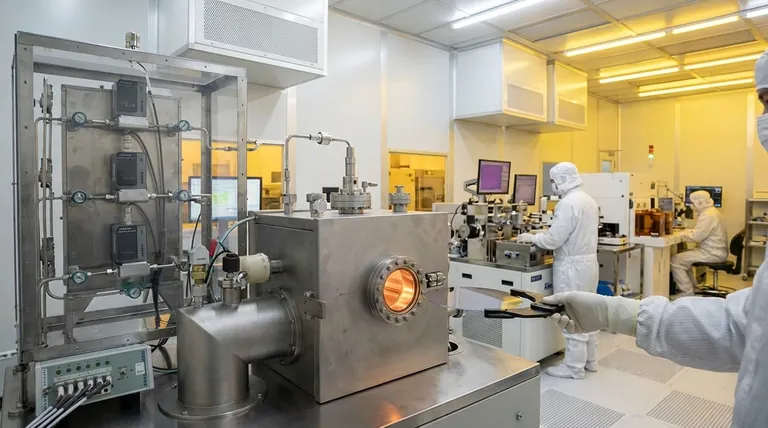
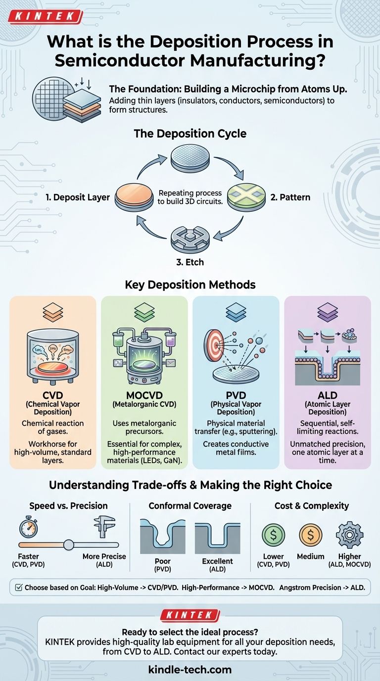
In semiconductor manufacturing, deposition is the foundational process of adding thin layers of material onto a silicon wafer. These layers are the fundamental building blocks—the insulators, conductors, and semiconductors—that are patterned and etched to create the intricate, three-dimensional structures of a microchip.
Deposition is not a single action but a family of highly controlled techniques for building a chip layer by layer. The choice of technique is a critical engineering decision, balancing the need for speed, precision, and material properties for each specific step in the fabrication process.
The Purpose of Deposition: Building a Microchip from the Atoms Up
Deposition is a core step in the repeating cycle of semiconductor fabrication. Engineers repeatedly deposit a layer, pattern it using photolithography, and then etch away unwanted material to form circuits.
From Insulators to Conductors
Deposition is used to add all types of materials required for a functioning transistor. This includes dielectric films that insulate wires from each other, conductive metal films that form the wires and interconnects, and crystalline semiconductor films that form the transistor channels.
Creating Atomically Precise Structures
The layers being deposited are incredibly thin, often measured in angstroms or nanometers—sometimes just a few atoms thick. The quality of this deposition process directly impacts the final performance, power consumption, and reliability of the chip.
Key Deposition Methods and Their Roles
Different methods are used depending on the material being deposited and the required characteristics of the film, such as its thickness uniformity and how well it covers complex, non-flat surfaces.
Chemical Vapor Deposition (CVD)
CVD is a workhorse of the industry. It involves flowing precursor gases into a chamber where they react on the hot wafer surface, leaving behind a solid thin film. The "vapor" in the name refers to these gaseous chemical precursors.
Focus on MOCVD
A specialized and significant subset of CVD is Metalorganic Chemical Vapor Deposition (MOCVD). It uses metalorganic compounds as precursors and is essential for creating high-quality, complex semiconductor materials for devices like LEDs and high-power transistors.
MOCVD is valued for its ability to achieve high precision and material flexibility in high-volume production, making it a cost-efficient method for advanced chip designs.
Physical Vapor Deposition (PVD)
Unlike the chemical reactions of CVD, PVD methods physically transfer material onto the wafer. A common technique is sputtering, where a target made of the desired material is bombarded with ions, knocking atoms loose that then land on and coat the wafer.
Atomic Layer Deposition (ALD)
ALD is the most precise method available. It builds material by exposing the wafer to sequential, self-limiting chemical reactions, depositing exactly one atomic layer at a time. This unparalleled control is critical for creating the gate oxides and other ultra-thin films in modern, cutting-edge transistors.
Understanding the Trade-offs
No single deposition method is perfect for every application. The choice always involves balancing competing factors.
Speed vs. Precision
There is a direct trade-off between how fast a layer can be grown and how precisely it can be controlled. Processes like CVD are generally much faster and have higher throughput than ALD, which is inherently slow due to its layer-by-layer nature.
Conformal Coverage
Conformality is the ability of a film to coat evenly over complex, three-dimensional topography. ALD provides near-perfect conformality, which is essential for lining deep trenches and complex shapes in modern FinFET transistors. CVD has good conformality, while PVD is a line-of-sight process and struggles to evenly coat vertical sidewalls.
Cost and Complexity
The equipment required for these processes varies dramatically in cost and complexity. ALD and MOCVD systems are highly sophisticated and expensive, justified only when the utmost precision or specific material properties are required. PVD and standard CVD systems can be more cost-effective for less critical layers.
Making the Right Choice for Your Goal
Selecting a deposition technique is dictated by the specific requirements of the layer being built.
- If your primary focus is high-volume manufacturing of standard insulating or metal layers: Chemical Vapor Deposition (CVD) and Physical Vapor Deposition (PVD) often provide the best balance of speed, cost, and quality.
- If your primary focus is creating high-performance compound semiconductors like GaN or GaAs: Metalorganic CVD (MOCVD) is the industry standard for its precision and ability to control complex material composition.
- If your primary focus is building cutting-edge logic transistors with angstrom-level precision: Atomic Layer Deposition (ALD) is essential for its unmatched thickness control and ability to conformally coat complex 3D structures.
Ultimately, mastering deposition is about selecting the right tool to precisely construct each specific layer of a semiconductor device.
Summary Table:
| Method | Full Name | Key Characteristic | Primary Use Case |
|---|---|---|---|
| CVD | Chemical Vapor Deposition | Chemical reaction of gases on wafer surface | High-volume manufacturing of standard layers |
| MOCVD | Metalorganic Chemical Vapor Deposition | Uses metalorganic precursors for complex materials | LEDs, high-power transistors (GaN, GaAs) |
| PVD | Physical Vapor Deposition | Physical transfer of material (e.g., sputtering) | Conductive metal layers |
| ALD | Atomic Layer Deposition | Deposits one atomic layer at a time | Ultra-thin, precise films for advanced transistors |
Ready to select the ideal deposition process for your semiconductor fabrication? The right equipment is critical for achieving the precise material properties, conformality, and throughput your project demands. KINTEK specializes in high-quality lab equipment and consumables for all your deposition needs, from robust CVD systems to sophisticated ALD solutions. Let our experts help you build the foundation for your next-generation microchips. Contact our team today to discuss your specific application requirements.
Visual Guide
Related Products
- RF PECVD System Radio Frequency Plasma-Enhanced Chemical Vapor Deposition RF PECVD
- HFCVD Machine System Equipment for Drawing Die Nano-Diamond Coating
- Chemical Vapor Deposition CVD Equipment System Chamber Slide PECVD Tube Furnace with Liquid Gasifier PECVD Machine
- 915MHz MPCVD Diamond Machine Microwave Plasma Chemical Vapor Deposition System Reactor
- Customer Made Versatile CVD Tube Furnace Chemical Vapor Deposition Chamber System Equipment
People Also Ask
- What is the role of RF-PECVD in VFG preparation? Mastering Vertical Growth and Surface Functionality
- What is plasma enhanced chemical vapour deposition process? Unlock Low-Temperature, High-Quality Thin Films
- What is plasma chemical vapor deposition? A Low-Temperature Thin Film Coating Solution
- How does Radio Frequency Enhanced Plasma Chemical Vapour Deposition (RF-PECVD) work? Learn the Core Principles
- What is plasma enhanced chemical vapour deposition PECVD used for? Enable Low-Temp Thin Films for Electronics & Solar


