In essence, electron beam physical vapor deposition (E-beam PVD) is a vacuum coating process used to apply extremely thin, high-purity films onto a surface. It works by using a high-energy beam of electrons to heat a source material until it evaporates. This vapor then travels through the vacuum and condenses onto a cooler target object, known as a substrate, forming a uniform coating.
The core principle of E-beam PVD is its ability to efficiently vaporize a wide range of materials, including those with very high melting points. This makes it a versatile and rapid method for producing high-quality thin films for industries ranging from aerospace to optics.
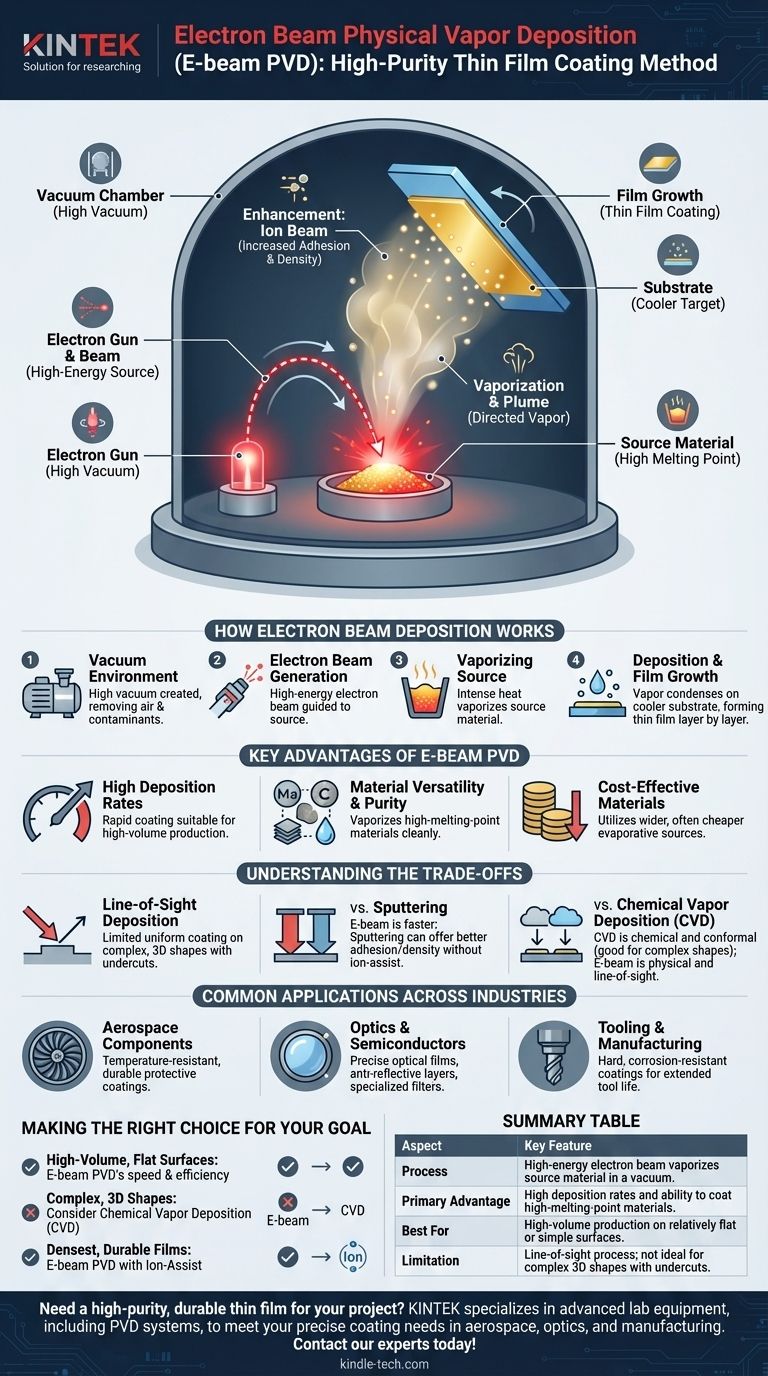
How Electron Beam Deposition Works
The E-beam PVD process is a sophisticated technique that relies on precise control over a series of physical events within a high-vacuum chamber.
The Vacuum Environment
First, both the substrate and the source material are placed inside a chamber where a high vacuum is created. This vacuum is critical because it removes air and other particles, ensuring the evaporated material can travel to the substrate without colliding with contaminants.
Generating the Electron Beam
A beam of high-energy electrons is generated and magnetically guided toward the source material, which is held in a crucible. This beam is the "engine" of the process.
Vaporizing the Source Material
The focused electron beam strikes the source material (often in powder or granular form) with intense energy. This energy rapidly heats the material past its boiling point, causing it to turn directly into a vapor.
Deposition and Film Growth
The resulting vapor expands throughout the vacuum chamber, traveling in a straight line. When the vapor particles hit the relatively cool substrate, they condense back into a solid state. Through precise computer control of factors like vacuum levels and substrate rotation, this condensation builds up layer by layer into a thin film of a predetermined thickness.
Enhancement with Ion Beams
For applications requiring maximum durability, the process can be enhanced with an ion beam. This secondary beam bombards the growing film with ions, increasing its adhesion and resulting in a denser, more robust coating with less internal stress.
Key Advantages of the E-Beam PVD Method
E-beam PVD is chosen over other methods for several distinct operational and economic benefits.
High Deposition Rates
Compared to techniques like magnetron sputtering, E-beam PVD can deposit material much more quickly. This speed makes it highly suitable for high-volume commercial production where efficiency is paramount.
Material Versatility and Purity
The process is capable of vaporizing materials with extremely high melting points, which are difficult to handle with other methods. Because the energy is transferred directly to the source material, the process is very clean, resulting in high-purity films.
Cost-Effective Materials
E-beam PVD can utilize a wide array of evaporative source materials that are often less expensive than the specialized targets required for other processes like sputtering.
Understanding the Trade-offs
No single technology is perfect for every application. Understanding the limitations of E-beam PVD is critical for making an informed decision.
Line-of-Sight Deposition
The primary limitation of E-beam PVD is that it is a line-of-sight process. The vapor travels in a straight line from the source to the substrate. This makes it challenging to uniformly coat complex, three-dimensional shapes with undercuts or hidden surfaces.
Comparison with Sputtering
While E-beam is often faster, sputtering can sometimes offer better film adhesion and density without the need for an ion-assist source. The choice often comes down to the specific material, desired film properties, and production volume.
Comparison with Chemical Vapor Deposition (CVD)
CVD is a chemical process, not a physical one, and it excels at creating highly conformal coatings. This means it can uniformly cover very rough or complex surfaces where E-beam PVD would fail. CVD also typically operates at lower vacuum levels.
Common Applications Across Industries
The unique capabilities of E-beam PVD have made it essential in several high-tech fields.
Aerospace Components
The technique is used to apply dense, temperature-resistant coatings that protect engine parts and other components from extreme heat and wear, enhancing durability.
Optics and Semiconductors
It is used to apply precise optical films, such as anti-reflective coatings on lenses or specialized filters for solar panels and semiconductor manufacturing.
Tooling and Manufacturing
Hard, corrosion-resistant coatings are applied to cutting tools and industrial components, significantly extending their operational life in harsh environments.
Making the Right Choice for Your Goal
Selecting the correct deposition technology depends entirely on your project's specific requirements for material, geometry, and performance.
- If your primary focus is high-volume production of films on relatively flat surfaces: E-beam PVD's speed and material efficiency make it an excellent choice.
- If your primary focus is coating complex, three-dimensional shapes uniformly: You should investigate a non-line-of-sight method like Chemical Vapor Deposition (CVD).
- If your primary focus is creating the densest, most durable films possible: Consider E-beam PVD enhanced with an ion-assist source to maximize adhesion and robustness.
By understanding its fundamental principles and trade-offs, you can effectively leverage the power and precision of electron beam PVD for your specific application.
Summary Table:
| Aspect | Key Feature |
|---|---|
| Process | High-energy electron beam vaporizes source material in a vacuum. |
| Primary Advantage | High deposition rates and ability to coat high-melting-point materials. |
| Best For | High-volume production on relatively flat or simple surfaces. |
| Limitation | Line-of-sight process; not ideal for complex 3D shapes with undercuts. |
Need a high-purity, durable thin film for your project? KINTEK specializes in advanced lab equipment, including PVD systems, to meet the precise coating needs of laboratories in aerospace, optics, and manufacturing. Our solutions ensure material versatility and high deposition rates for your most demanding applications. Contact our experts today to discuss how we can enhance your coating process!
Visual Guide
Related Products
- Electron Beam Evaporation Coating Oxygen-Free Copper Crucible and Evaporation Boat
- E Beam Crucibles Electron Gun Beam Crucible for Evaporation
- Electron Beam Evaporation Coating Gold Plating Tungsten Molybdenum Crucible for Evaporation
- Molybdenum Tungsten Tantalum Evaporation Boat for High Temperature Applications
- Chemical Vapor Deposition CVD Equipment System Chamber Slide PECVD Tube Furnace with Liquid Gasifier PECVD Machine
People Also Ask
- What is the voltage of e-beam evaporation? Achieve Precise Thin-Film Deposition
- What is the deposition rate of e-beam evaporation? Control Thin Film Quality and Speed
- How is an electron beam evaporator cooled during deposition? Essential Thermal Management for Stable Processes
- What is e-beam evaporation? Achieve High-Purity Thin Film Deposition for Your Lab
- What is e-beam evaporation used for? Precision Coating for Optics, Aerospace & Electronics


