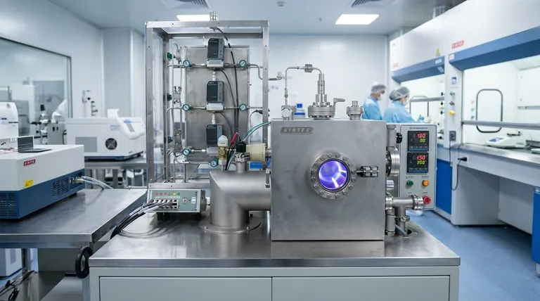
At its core, magnetron sputtering is a highly controlled vacuum coating process used to deposit exceptionally thin, high-performance films of material onto a surface. It operates by creating a plasma and using a magnetic field to eject atoms from a source material (the "target") which then land on and coat the desired object (the "substrate"). This atom-by-atom deposition allows for immense precision and results in films with superior purity, density, and adhesion.
Magnetron sputtering is not merely a method for applying a coating; it is a technique for engineering a new surface. It leverages plasma physics and magnetic fields to construct an atomic-level film, fundamentally altering a substrate's properties for advanced applications.
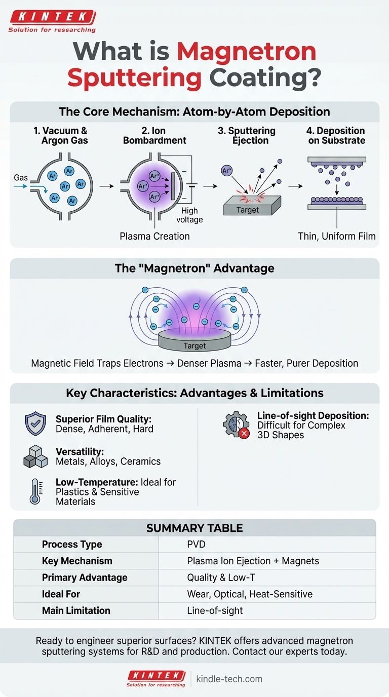
The Core Mechanism: From Plasma to Film
To understand magnetron sputtering, it's best to visualize it as a four-step sequence occurring inside a vacuum chamber.
Step 1: Creating a Plasma Vacuum
The process begins by placing the substrate to be coated and the target material into a chamber and removing the air to create a high vacuum.
A small amount of an inert gas, typically Argon (Ar), is then introduced into the chamber. This gas provides the atoms that will be used for the bombardment.
Step 2: Ion Bombardment
A high voltage is applied to the target, causing it to become a cathode (negative electrode). This electrical energy ignites the argon gas, stripping electrons from the argon atoms and creating a plasma—a glowing, ionized gas composed of positive argon ions (Ar+) and free electrons.
Because opposite charges attract, the positively charged argon ions are aggressively accelerated toward the negatively charged target.
Step 3: The "Sputtering" Ejection
When these high-energy argon ions collide with the target, they transfer their momentum, physically knocking atoms or molecules loose from the target material.
This atomic-level ejection is the "sputtering" effect. These dislodged particles fly away from the target with significant kinetic energy.
Step 4: Deposition on the Substrate
The sputtered atoms travel through the vacuum chamber and strike the substrate, which is strategically placed to intercept them.
Upon impact, they condense and build up on the substrate's surface, forming a thin, uniform, and highly adherent film.
The "Magnetron" Advantage: Enhancing Efficiency
Standard sputtering works, but adding magnets transforms the process, making it dramatically more efficient and controllable. This is the "magnetron" in magnetron sputtering.
Trapping Electrons with Magnets
A powerful magnetic field is strategically applied behind the sputtering target. This field is designed to trap the free electrons from the plasma in a concentrated region near the target's surface.
Creating a Denser Plasma
By holding electrons near the target, the magnetic field dramatically increases the probability that they will collide with and ionize neutral argon atoms.
This creates a much denser, more intense plasma directly in front of the target without requiring higher gas pressure or voltage.
The Result: Faster, More Stable Deposition
A denser plasma means more argon ions are available to bombard the target. This results in a significantly higher sputtering rate and faster film deposition.
Furthermore, this efficiency allows the process to run at lower pressures, meaning the sputtered atoms encounter fewer gas collisions on their way to the substrate, resulting in higher-purity films.
Understanding the Trade-offs and Key Characteristics
Like any technical process, magnetron sputtering has distinct strengths and limitations that make it ideal for some applications and less suitable for others.
Advantage: Superior Film Quality
The high kinetic energy of the sputtered atoms results in films that are extremely dense, well-adhered, and often harder than films produced by other methods. This is why it's chosen for wear-resistant and protective coatings.
Advantage: Versatility of Materials
The process is purely physical (momentum transfer), not chemical or thermal. This allows for the deposition of a vast range of materials, including pure metals, alloys, and even ceramic compounds that are difficult to evaporate.
Advantage: Low-Temperature Process
While the plasma is hot, the sputtered atoms themselves do not transfer significant heat to the substrate. This makes magnetron sputtering ideal for coating heat-sensitive materials like plastics, polymers, or biological specimens for electron microscopy.
Limitation: Line-of-Sight Deposition
Sputtered atoms travel in a straight line from the target to the substrate. This means it is very difficult to uniformly coat complex, three-dimensional shapes with hidden or internal surfaces without sophisticated part manipulation.
Making the Right Choice for Your Goal
Selecting a coating technology depends entirely on your end goal. Magnetron sputtering is a powerful tool when its specific advantages align with your project's requirements.
- If your primary focus is high-performance and durable coatings: Magnetron sputtering offers exceptional hardness, density, and adhesion for applications requiring wear resistance and longevity.
- If your primary focus is coating heat-sensitive materials: The low-temperature nature of the process protects delicate substrates like polymers or biological samples from thermal damage.
- If your primary focus is depositing complex alloys or compounds: Sputtering can accurately reproduce the composition of the source target in the final film, something other methods struggle with.
- If your primary focus is coating complex, non-visible surfaces: You should consider alternative, non-line-of-sight methods like chemical vapor deposition (CVD) or electroplating.
Ultimately, magnetron sputtering empowers engineers and scientists to construct materials atom by atom, building high-performance surfaces from the ground up.
Summary Table:
| Feature | Description |
|---|---|
| Process Type | Physical Vapor Deposition (PVD) |
| Key Mechanism | Ejection of target atoms via plasma ion bombardment, enhanced by magnetic fields |
| Primary Advantage | Superior film quality (density, adhesion, purity) and low-temperature operation |
| Ideal For | Wear-resistant coatings, optical coatings, semiconductor layers, coating heat-sensitive substrates |
| Main Limitation | Line-of-sight deposition, making complex 3D coating challenging |
Ready to engineer superior surfaces with precision?
KINTEK specializes in advanced lab equipment, including magnetron sputtering systems designed for reliability and high-performance results. Whether your focus is on R&D, semiconductor fabrication, or creating durable protective coatings, our solutions help you achieve exceptional film quality and process control.
Let's discuss your specific coating challenges and goals. Contact our experts today to find the perfect sputtering solution for your laboratory.
Visual Guide
Related Products
- Electron Beam Evaporation Coating Gold Plating Tungsten Molybdenum Crucible for Evaporation
- Electron Beam Evaporation Coating Oxygen-Free Copper Crucible and Evaporation Boat
- Custom PTFE Teflon Parts Manufacturer for Magnetic Stirring Bar
- Infrared Transmission Coating Sapphire Sheet Substrate Window
People Also Ask
- What is the container that holds the metal source material called in e-beam evaporation? Ensure Purity and Quality in Your Thin-Film Deposition
- What is the voltage of e-beam evaporation? Achieve Precise Thin-Film Deposition
- What are the applications of e-beam evaporation? Achieve High-Purity Coatings for Optics & Electronics
- What materials are used in electron beam evaporation? Master High-Purity Thin Film Deposition
- What is the process of e-beam coating? Achieve High-Purity, Precise Thin Films for Your Lab


