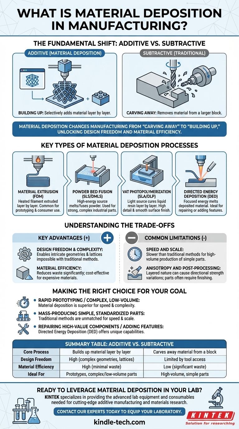
At its core, material deposition is a manufacturing process where an object is built by selectively adding material, typically layer by layer, from a digital design file. This method is the fundamental principle behind what is more commonly known as additive manufacturing or 3D printing. It is a direct contrast to traditional subtractive methods, where material is removed from a larger block to create the final shape.
The crucial shift to understand is that material deposition changes manufacturing from a process of "carving away" to one of "building up." This fundamental difference unlocks unprecedented design freedom and material efficiency, but it also introduces a new set of production considerations.

The Fundamental Shift: Additive vs. Subtractive
To grasp the importance of material deposition, it's essential to compare it with the manufacturing paradigm it challenges.
The Traditional Approach: Subtractive Manufacturing
Traditional manufacturing typically starts with a solid block of material, such as metal, plastic, or wood.
Tools like CNC mills, lathes, and drills then cut, grind, or drill away the excess material to reveal the final part. This is analogous to a sculptor carving a statue from a block of marble.
The Modern Paradigm: Additive Manufacturing
Material deposition, the engine of additive manufacturing, starts with nothing.
It systematically adds material only where it is needed to form the object, layer by microscopic layer. This is more like building an object with LEGO bricks, but on an incredibly fine scale.
Key Types of Material Deposition Processes
Material deposition is not a single technology but a category of processes, each with unique strengths and applications.
Material Extrusion (FDM)
This is the most widely recognized form of 3D printing. A thermoplastic filament is heated and extruded through a nozzle, building the object layer by layer as the material cools and solidifies. It is common for prototyping and consumer-grade applications.
Powder Bed Fusion (SLS/DMLS)
In this process, a high-energy source like a laser or electron beam selectively melts and fuses fine particles of plastic or metal powder in a bed. After each layer is fused, a new layer of powder is spread over the top. This is used for creating strong, complex industrial parts.
Vat Photopolymerization (SLA/DLP)
This method uses a light source—a laser (SLA) or a digital projector (DLP)—to selectively cure a liquid photopolymer resin in a vat. The object is built layer by layer as the liquid hardens into a solid. It's known for producing parts with very high detail and smooth surface finishes.
Directed Energy Deposition (DED)
DED uses a focused thermal energy source, such as a laser or electron beam, to melt material as it is being deposited. Often used with metal powder or wire, this technique is frequently employed for repairing or adding features to existing large-scale components, like turbine blades.
Understanding the Trade-offs
Like any technology, material deposition comes with distinct advantages and limitations that define its ideal use cases.
Key Advantage: Design Freedom & Complexity
Deposition processes can create intricate internal geometries, lattice structures, and organic shapes that are impossible or prohibitively expensive to produce with traditional subtractive methods.
Key Advantage: Material Efficiency
Since material is only added where it is needed, waste is drastically reduced compared to carving a small part from a large block of raw material. This is especially cost-effective when using expensive materials like titanium.
Common Limitation: Speed and Scale
For high-volume production of relatively simple parts, traditional methods like injection molding are significantly faster and more cost-effective per unit. Layer-by-layer deposition can be a slow process.
Common Limitation: Anisotropy and Post-Processing
The layered nature of deposited parts can create directional variations in strength, known as anisotropy. Many parts also require post-processing steps like sanding, polishing, or heat treatment to achieve the desired surface finish and mechanical properties.
Making the Right Choice for Your Goal
The best manufacturing method depends entirely on your project's specific constraints and objectives.
- If your primary focus is rapid prototyping or creating highly complex, low-volume parts: Material deposition is almost always the superior choice due to its speed in producing initial designs and its ability to handle complexity.
- If your primary focus is mass-producing millions of simple, standardized parts at the lowest possible cost: Traditional subtractive or formative manufacturing (e.g., molding) remains the industry standard for its unmatched speed and scale.
- If your primary focus is repairing high-value metal components or adding custom features to existing parts: Directed Energy Deposition (DED) offers unique capabilities that other methods cannot match.
Understanding material deposition is no longer a niche skill; it is a fundamental pillar of modern engineering, design, and manufacturing.
Summary Table:
| Aspect | Additive (Material Deposition) | Subtractive (Traditional) |
|---|---|---|
| Core Process | Builds up material layer by layer | Carves away material from a block |
| Design Freedom | High (complex geometries, lattices) | Limited by tool access |
| Material Efficiency | High (minimal waste) | Low (significant waste) |
| Ideal For | Prototypes, complex/low-volume parts | High-volume, simple parts |
Ready to leverage material deposition in your lab?
KINTEK specializes in providing the advanced lab equipment and consumables needed for cutting-edge additive manufacturing and materials research. Whether you are developing new materials for 3D printing or analyzing the properties of deposited layers, our solutions support your innovation.
Contact our experts today to discuss how we can equip your laboratory for the future of manufacturing.
Visual Guide
Related Products
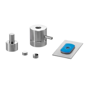
- Lab Infrared Press Mold
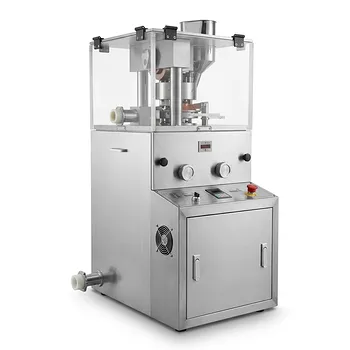
- Single Punch Manual Tablet Press Machine TDP Tablet Punching Machine
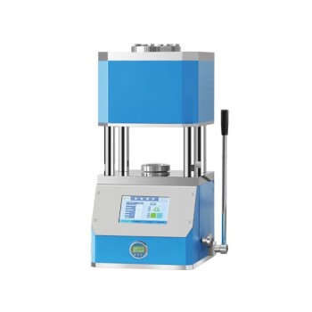
- Manual High Temperature Heated Hydraulic Press Machine with Heated Plates for Lab
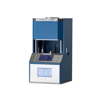
- Automatic High Temperature Heated Hydraulic Press Machine with Heated Plates for Lab
- Single Punch Electric Tablet Press Machine Laboratory Powder Tablet Punching TDP Tablet Press
People Also Ask
- What is a press mold used for? Achieve Repeatable Precision and Efficiency
- What is the function of press molds during the preparation of SiCf/Ti-43Al-9V composites? Achieve Structural Precision
- What is the purpose of specialized pressure devices in sulfide solid-state batteries? Ensure Chemo-Mechanical Stability
- What is the process of mold press? A Step-by-Step Guide to Compression Molding
- What is the press mould method? A Guide to Consistent, Detailed Ceramic Forms