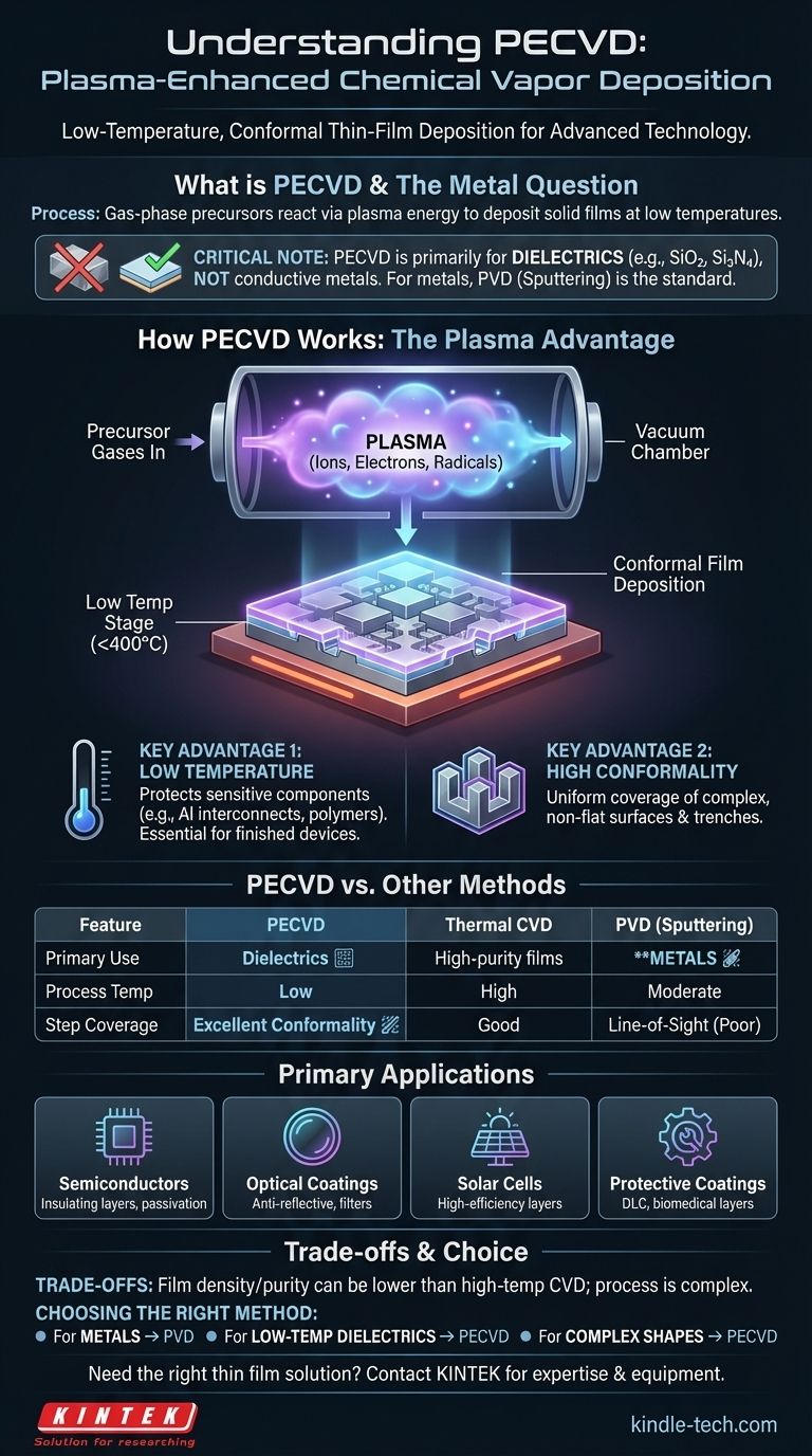
In short, Plasma-Enhanced Chemical Vapor Deposition (PECVD) is a process used to deposit thin films from a gas state onto a solid substrate at low temperatures. It utilizes plasma to provide the energy for chemical reactions, distinguishing it from conventional Chemical Vapor Deposition (CVD) which relies on high heat. While you asked about metal deposition, it's critical to understand that PECVD is overwhelmingly used for depositing dielectric and semiconducting materials, not conductive metals.
The core advantage of PECVD is its ability to create high-quality, uniform films at temperatures low enough to avoid damaging sensitive electronic components. This makes it an essential tool in modern semiconductor and nanofabrication, where other high-temperature methods are not viable.
How PECVD Works: The Role of Plasma
At its heart, PECVD is a refined version of chemical vapor deposition. The "plasma-enhanced" aspect is the key innovation that defines its capabilities and applications.
From Gas to Solid Film
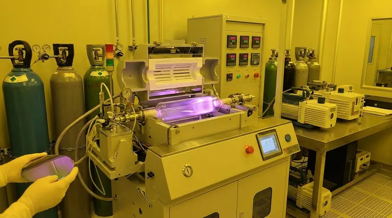
Like all CVD processes, PECVD begins with precursor gases being introduced into a vacuum chamber containing the substrate (e.g., a silicon wafer). The goal is to make these gases react and deposit a solid film onto the substrate's surface.
The "Plasma-Enhanced" Advantage
Instead of using high temperatures (often >600°C) to drive this reaction, PECVD uses an electric field to ionize the gases, creating a plasma. This plasma is a high-energy state of matter containing ions and electrons.
These high-energy electrons collide with the precursor gas molecules, breaking them into reactive radicals. This provides the necessary energy for the chemical reactions to occur on the substrate surface, but without needing to heat the substrate itself to extreme temperatures.
Why Plasma Enables Low Temperatures
The ability to initiate reactions without high heat is the single most important feature of PECVD. It allows for the deposition of films on top of fully or partially fabricated devices that contain materials, such as aluminum interconnects, which would be damaged or destroyed by the high temperatures of thermal CVD.
The Efficiency of the Process
The electric field used to generate the plasma is typically strongest near the substrate (the cathode). This concentrates the chemical reactions directly on the surface where deposition is desired, increasing the deposition rate and minimizing wasted material on the chamber walls.
PECVD vs. Other Deposition Methods
Understanding PECVD requires seeing where it fits in the landscape of thin-film technologies, particularly in contrast to thermal CVD and Physical Vapor Deposition (PVD).
The Temperature Advantage Over Thermal CVD
The primary competitor within the CVD family is Low-Pressure CVD (LPCVD), a thermal process. While LPCVD can produce very high-purity films, its high-temperature requirement makes it unsuitable for many steps in advanced integrated circuit manufacturing. PECVD fills this critical low-temperature gap.
The Coverage Advantage Over PVD
PVD methods, like sputtering, are fundamentally "line-of-sight." The source material travels in a straight line to the substrate. This makes it difficult to uniformly coat complex, non-flat surfaces. Because PECVD uses a gas that fills the entire chamber, it can deposit a highly conformal film that uniformly covers intricate topographies.
Understanding Primary Applications (and the Metal Question)
PECVD's unique low-temperature, high-conformality profile makes it the go-to process for specific, critical applications.
Core Use Case: Semiconductor Manufacturing
This is PECVD's main domain. It is widely used to deposit dielectric (insulating) films like silicon dioxide (SiO₂) and silicon nitride (Si₃N₄). These layers are used to electrically isolate conductive pathways, act as capacitor dielectrics, and provide a final protective "passivation" layer over the completed chip.
Beyond Microelectronics
The same principles apply to other high-tech fields. PECVD is used to create anti-reflective coatings for optics and sunglasses, manufacture high-efficiency solar cells, and deposit hard, protective coatings like Diamond-Like Carbon (DLC) on mechanical parts. It is also used for hydrophobic coatings and creating protective layers for medical implants.
The Question of Metal Deposition
While you asked about metals, PVD methods like sputtering are the dominant industry standard for depositing metallic films like aluminum, copper, and titanium. The precursor chemistries and plasma conditions for PECVD are highly optimized for silicon-based dielectrics and other non-metallic compounds. While some specialized PECVD metal depositions exist in research, for commercial manufacturing, PVD is the process for metals, and PECVD is the process for dielectrics.
Understanding the Trade-offs
No technology is without limitations. Objectivity requires acknowledging the trade-offs involved with choosing PECVD.
Film Quality Considerations
Because PECVD is a lower-temperature process, the deposited films can sometimes have lower density and higher hydrogen content compared to films from high-temperature LPCVD. This can affect electrical properties and may not be suitable for all applications, but for its intended purpose, the quality is more than sufficient.
Process Complexity
Managing a plasma process adds a layer of complexity. Controlling gas flow, pressure, RF power, and frequency requires sophisticated equipment and process control compared to some simpler PVD or thermal methods.
Choosing the Right Deposition Method
Your choice of technology should be driven entirely by the material you need to deposit and the constraints of your substrate.
- If your primary focus is depositing conductive metal layers (like interconnects): You should use a PVD technique like sputtering, which is the established industry standard for high-quality metal films.
- If your primary focus is depositing high-quality insulating layers on temperature-sensitive devices: PECVD is the ideal choice due to its low-temperature processing capability.
- If your primary focus is coating complex 3D shapes with a uniform protective or optical film: PECVD offers a significant advantage over line-of-sight PVD methods due to its excellent conformality.
Ultimately, selecting the correct deposition method is about matching the tool to the specific engineering problem you need to solve.
Summary Table:
| Feature | PECVD | Thermal CVD / LPCVD | PVD (Sputtering) |
|---|---|---|---|
| Primary Use | Dielectrics (SiO₂, Si₃N₄) | High-purity films | Metal Deposition (Al, Cu, Ti) |
| Process Temperature | Low (< 400°C) | High (> 600°C) | Moderate |
| Step Coverage | Excellent Conformality | Good | Line-of-Sight (Poor) |
| Ideal For | Temperature-sensitive devices, complex 3D shapes | High-temperature substrates | Flat surfaces, metal interconnects |
Need to Deposit the Right Thin Film for Your Application?
Whether your project requires the low-temperature, conformal coatings of PECVD for sensitive electronics or high-quality metal layers from PVD sputtering, KINTEK has the expertise and equipment to meet your laboratory's specific needs.
Contact us today using the form below to discuss how our solutions can enhance your research and development process.
Visual Guide
Related Products
- Inclined Rotary Plasma Enhanced Chemical Vapor Deposition PECVD Equipment Tube Furnace Machine
- Chemical Vapor Deposition CVD Equipment System Chamber Slide PECVD Tube Furnace with Liquid Gasifier PECVD Machine
- Inclined Rotary Plasma Enhanced Chemical Vapor Deposition PECVD Equipment Tube Furnace Machine
- RF PECVD System Radio Frequency Plasma-Enhanced Chemical Vapor Deposition RF PECVD
- Multi Heating Zones CVD Tube Furnace Machine Chemical Vapor Deposition Chamber System Equipment
People Also Ask
- What is plasma enhanced chemical vapour deposition PECVD used for? Enable Low-Temp Thin Films for Electronics & Solar
- What are the benefits of plasma enhanced CVD? Achieve High-Quality, Low-Temperature Film Deposition
- What is plasma enhanced chemical vapor deposition PECVD equipment? A Guide to Low-Temperature Thin Film Deposition
- Why is a PECVD system required for vertical graphene synthesis? Master Directional Control for 3D Nanostructures
- How does PECVD facilitate Ru-C nanocomposite films? Precision Low-Temperature Thin Film Synthesis


