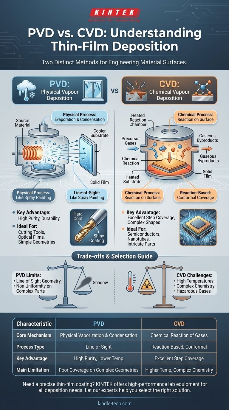
To be precise, the term you're using likely refers to two distinct but related families of techniques: Physical Vapour Deposition (PVD) and Chemical Vapour Deposition (CVD). Both are used to apply extremely thin films of material onto a surface, but they achieve this result through fundamentally different mechanisms. PVD is a physical process where a material is vaporized and then condenses onto the target, while CVD is a chemical process where gases react to form a solid film on the target surface.
The core difference is simple: PVD is like freezing steam back into ice on a cold window—a change of physical state. CVD is like rust forming on metal—a chemical reaction that creates a new material on the surface.
The Core Mechanism: How Each Process Works
To choose the right method, you must first understand how each one builds a film at the atomic level. Their "how" directly determines their "what" and "where."
Physical Vapour Deposition (PVD): A Line-of-Sight Process
In PVD, a solid or liquid source material is placed in a vacuum chamber and vaporized. This is done by physical means, such as heating it until it evaporates or bombarding it with ions.
These vaporized atoms travel in a straight line through the vacuum until they strike the target object, known as the substrate. Upon hitting the cooler substrate, the atoms condense and form a thin, solid film.
Because the atoms travel in a straight line, PVD is considered a line-of-sight technique. Imagine spray painting an object; the paint only covers the surfaces it can directly see.
Chemical Vapour Deposition (CVD): A Reaction-Based Process
CVD does not start with a solid source material. Instead, one or more volatile precursor gases are introduced into a reaction chamber containing the substrate.
The substrate is typically heated, providing the energy needed to trigger a chemical reaction between the gases on or near its surface.
The result of this reaction is a solid material that deposits onto the substrate, forming the desired film. Other gaseous byproducts from the reaction are simply pumped out of the chamber.
Key Characteristics and Applications
The different mechanisms of PVD and CVD make them suitable for very different applications.
When to Choose PVD: Durability and High Purity
PVD excels at creating coatings that are extremely hard, dense, and resistant to high temperatures and corrosion.
Common applications include applying protective coatings to cutting tools, creating durable finishes on components, and depositing thin optical films for semiconductors and solar panels. Aerospace companies use it to enhance the durability of parts exposed to extreme environments.
When to Choose CVD: Complexity and Conformal Coverage
CVD's primary advantage is its ability to create highly conformal coatings. Because the deposition is driven by a chemical reaction with a gas, it can uniformly coat complex, three-dimensional shapes and internal surfaces.
This makes it indispensable in the semiconductor industry for depositing intricate layers on microchips. It is also used to grow materials like carbon nanotubes and create a wide variety of high-purity metal, alloy, and ceramic layers.
Understanding the Trade-offs
Neither method is universally superior. The choice involves clear, well-defined trade-offs based on the material, the substrate's shape, and the desired outcome.
The Limits of PVD: Geometry Matters
The line-of-sight nature of PVD is its biggest limitation. It struggles to evenly coat the interior of complex shapes or the "backside" of an object without complex rotation and repositioning. This can lead to non-uniform film thickness on intricate parts.
The Challenges of CVD: Chemistry and Temperature
CVD processes often require higher temperatures than PVD to initiate the necessary chemical reactions. This high heat can damage sensitive substrates, such as certain plastics or electronic components.
Additionally, the precursor gases can be toxic, expensive, or difficult to handle, and controlling the complex chemistry to achieve a specific film composition requires significant expertise.
Making the Right Choice for Your Goal
Selecting the correct deposition method requires matching the process characteristics to your end goal.
- If your primary focus is a hard, wear-resistant coating on a relatively simple surface: PVD is often the more direct and effective solution for applications like tools and flat components.
- If your primary focus is uniformly coating a complex, three-dimensional object: CVD's reaction-based nature provides the superior conformal coverage needed for parts like microchips.
- If your primary focus is depositing a pure material at lower temperatures: PVD generally operates at lower process temperatures and avoids the chemical byproducts inherent to CVD.
By understanding the fundamental difference between these physical and chemical pathways, you can select the precise technique to engineer materials at the atomic level.
Summary Table:
| Characteristic | PVD (Physical Vapour Deposition) | CVD (Chemical Vapour Deposition) |
|---|---|---|
| Core Mechanism | Physical vaporization and condensation | Chemical reaction of precursor gases |
| Process Type | Line-of-sight | Reaction-based, conformal |
| Typical Applications | Hard, durable coatings (tools, optics) | Uniform coatings on complex shapes (semiconductors) |
| Key Advantage | High purity, lower temperature | Excellent step coverage |
| Main Limitation | Poor coverage on complex geometries | Higher temperatures, complex chemistry |
Need to apply a precise thin-film coating? Choosing between PVD and CVD is critical for your project's success. At KINTEK, we specialize in providing high-performance lab equipment and consumables for all your deposition needs. Whether you require the durability of PVD coatings or the conformal coverage of CVD, our experts can help you select the right solution for your laboratory. Contact us today to discuss your specific application and enhance your research capabilities!
Visual Guide
Related Products
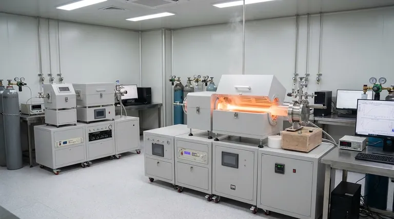
- Chemical Vapor Deposition CVD Equipment System Chamber Slide PECVD Tube Furnace with Liquid Gasifier PECVD Machine
- Customer Made Versatile CVD Tube Furnace Chemical Vapor Deposition Chamber System Equipment
- RF PECVD System Radio Frequency Plasma-Enhanced Chemical Vapor Deposition RF PECVD
- Microwave Plasma Chemical Vapor Deposition MPCVD Machine System Reactor for Lab and Diamond Growth
- HFCVD Machine System Equipment for Drawing Die Nano-Diamond Coating
People Also Ask
- What types of substrates are used in CVD to facilitate graphene films? Optimize Graphene Growth with the Right Catalyst
- What happens during deposition chemistry? Building Thin Films from Gaseous Precursors
- What is plasma enhanced chemical vapor deposition PECVD equipment? A Guide to Low-Temperature Thin Film Deposition
- How expensive is chemical vapor deposition? Understanding the True Cost of High-Performance Coating
- What is the chemical vapor deposition growth process? Build Superior Thin Films from the Atom Up


