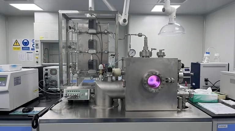
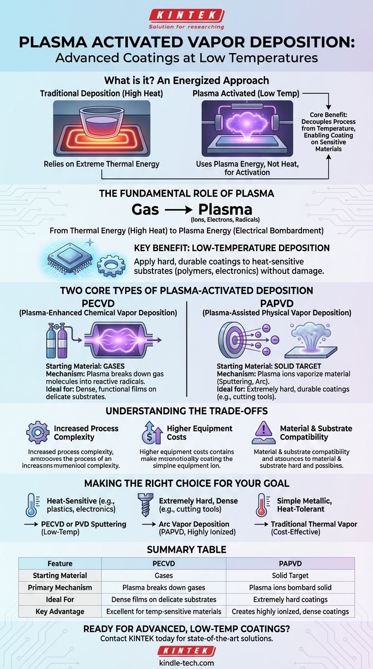
At its core, Plasma-Activated Vapor Deposition is a category of advanced coating techniques that uses an energized gas, or plasma, to create high-quality thin films. Instead of relying solely on high heat to drive the process, it uses the energy from plasma to break down precursor materials and deposit them onto a surface. This fundamental difference allows for deposition at significantly lower temperatures, expanding the range of materials and substrates that can be coated.
The central advantage of using plasma is that it provides the necessary "activation energy" for deposition without the extreme heat required by traditional methods. This decouples the process from temperature, enabling high-performance coatings on heat-sensitive materials like plastics and complex electronics.
The Fundamental Role of Plasma
To understand plasma-activated deposition, you must first understand why plasma is used at all. It serves as a highly efficient energy source that fundamentally changes how the coating process works.
What is Plasma in this Context?
Plasma is often called the fourth state of matter. It's a gas that has been energized to the point where its atoms are broken apart into a highly reactive mixture of ions, electrons, and neutral radicals.
In a deposition chamber, this cloud of energized particles becomes the primary tool for creating the coating, replacing the brute-force energy of high heat.
From Thermal Energy to Plasma Energy
Traditional methods like standard Chemical Vapor Deposition (CVD) or Thermal Vapor Deposition require high temperatures to work. This heat is needed to trigger chemical reactions or to boil a solid material into a vapor.
Plasma-activated processes achieve the same result electrically. The energetic particles within the plasma bombard the source material (a gas in PECVD, a solid in PVD), breaking it down and preparing it for deposition onto the substrate.
The Key Benefit: Low-Temperature Deposition
The most significant advantage of this approach is the ability to deposit films at much lower temperatures. This is critical because many advanced materials, such as polymers, plastics, and certain semiconductors, cannot withstand the high heat of conventional deposition processes.
By using plasma, you can apply hard, durable, or functional coatings to these temperature-sensitive substrates without damaging or melting them.
Two Core Types of Plasma-Activated Deposition
The term "plasma-activated" is broad and applies to two distinct families of deposition: Chemical and Physical. The key difference is the starting state of the material being deposited.
Plasma-Enhanced Chemical Vapor Deposition (PECVD)
In standard CVD, precursor gases react on a hot surface to form a solid film. The heat is the catalyst for the reaction.
PECVD uses plasma to energize those same precursor gases. The plasma breaks the gas molecules into highly reactive radicals, which then readily form a dense, high-quality film on the substrate, even at low temperatures.
Plasma-Assisted Physical Vapor Deposition (PAPVD)
In Physical Vapor Deposition (PVD), the source material starts as a solid. The goal is to turn it into a vapor that can coat a substrate. Plasma is an extremely effective way to do this.
Two common examples are:
- Sputtering: Plasma ions are accelerated to bombard a solid target, physically knocking atoms off its surface to be deposited.
- Arc Vapor Deposition: A high-current electric arc is used to vaporize the source material, creating a vapor with a very high percentage of ionized atoms, which leads to exceptionally dense and hard coatings.
Understanding the Trade-offs
While powerful, plasma-activated processes are not a universal solution. Their advantages come with specific considerations.
Increased Process Complexity
Introducing plasma adds another layer of control to the process. Managing the plasma's density, energy, and chemistry requires sophisticated equipment and precise control parameters to achieve repeatable, high-quality results.
Higher Equipment Costs
The power supplies, vacuum systems, and control mechanisms required to generate and sustain a stable plasma are generally more complex and expensive than the simple heating elements used in thermal deposition methods.
Material and Substrate Compatibility
While plasma vastly expands the range of coatable substrates, the highly reactive nature of the plasma itself can sometimes be detrimental. The process must be carefully tuned to ensure the plasma activates the deposition material without unintentionally damaging the substrate surface.
Making the Right Choice for Your Goal
Selecting the correct deposition method depends entirely on the material, the substrate, and the desired properties of the final coating.
- If your primary focus is coating heat-sensitive materials (e.g., plastics, electronics): A plasma-activated process like PECVD or PVD Sputtering is ideal due to its low-temperature operation.
- If your primary focus is creating an extremely hard, dense coating (e.g., on cutting tools): Arc Vapor Deposition (a PAPVD technique) is a superior choice because its highly ionized vapor creates exceptionally durable films.
- If your primary focus is a simple metallic coating on a heat-tolerant substrate: A traditional, non-plasma method like Thermal Vapor Deposition may be more cost-effective and sufficient.
Ultimately, plasma activation revolutionizes vapor deposition by providing a controlled, low-temperature path to producing advanced, high-performance coatings.
Summary Table:
| Feature | Plasma-Enhanced Chemical Vapor Deposition (PECVD) | Plasma-Assisted Physical Vapor Deposition (PAPVD) |
|---|---|---|
| Starting Material | Gases | Solid Target |
| Primary Mechanism | Plasma breaks down gas molecules into reactive radicals | Plasma ions bombard solid to vaporize material (e.g., Sputtering, Arc) |
| Ideal For | Dense, functional films on delicate substrates | Extremely hard, durable coatings (e.g., cutting tools) |
| Key Advantage | Excellent for temperature-sensitive materials | Creates highly ionized, dense coatings |
Ready to apply advanced, low-temperature coatings to your sensitive materials?
At KINTEK, we specialize in providing state-of-the-art lab equipment and consumables, including plasma-activated vapor deposition systems. Whether you are working with delicate polymers, complex electronics, or require ultra-hard coatings for industrial tools, our expertise can help you achieve superior results without compromising your substrate.
Contact us today to discuss how our solutions can enhance your laboratory's capabilities and drive your research forward. Get in touch with our experts now!
Visual Guide
Related Products
- RF PECVD System Radio Frequency Plasma-Enhanced Chemical Vapor Deposition RF PECVD
- Microwave Plasma Chemical Vapor Deposition MPCVD Machine System Reactor for Lab and Diamond Growth
- 915MHz MPCVD Diamond Machine Microwave Plasma Chemical Vapor Deposition System Reactor
- Chemical Vapor Deposition CVD Equipment System Chamber Slide PECVD Tube Furnace with Liquid Gasifier PECVD Machine
- Inclined Rotary Plasma Enhanced Chemical Vapor Deposition PECVD Equipment Tube Furnace Machine
People Also Ask
- Why is a Matching Network Indispensable in RF-PECVD for Siloxane Films? Ensure Stable Plasma and Uniform Deposition
- What is an example of PECVD? RF-PECVD for High-Quality Thin Film Deposition
- What is plasma enhanced chemical vapour deposition PECVD used for? Enable Low-Temp Thin Films for Electronics & Solar
- What is plasma enhanced chemical vapour deposition process? Unlock Low-Temperature, High-Quality Thin Films
- What is plasma chemical vapor deposition? A Low-Temperature Thin Film Coating Solution


