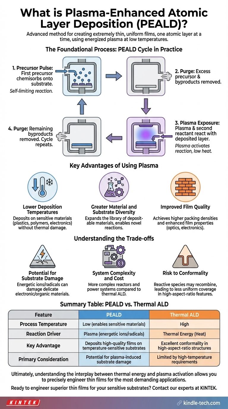
In essence, Plasma-Enhanced Atomic Layer Deposition (PEALD) is an advanced method for creating extremely thin, uniform films of material, one atomic layer at a time. It enhances the standard Atomic Layer Deposition (ALD) process by using an energized gas, or plasma, to drive the chemical reactions. This allows for high-quality film growth at much lower temperatures than traditional thermal methods require.
The central advantage of PEALD is its ability to decouple the reaction energy from thermal energy. By using plasma instead of high heat to activate the surface reactions, it enables the deposition of high-purity, dense films onto temperature-sensitive materials that would be damaged by other methods.
The Foundational Process: ALD vs. PEALD
To understand the value of PEALD, we must first distinguish it from the conventional process it is built upon: thermal ALD.
How Traditional (Thermal) ALD Works
Thermal Atomic Layer Deposition is a sequential process. It involves exposing a substrate to a series of different gas-phase chemical precursors, which are pulsed into the chamber one at a time.
Each pulse results in a self-limiting reaction that deposits a single, uniform monolayer of material. This provides precise thickness control, excellent uniformity, and the ability to perfectly coat complex, three-dimensional structures.
Introducing the Plasma Enhancement
Plasma enhancement replaces the high-temperature requirement of thermal ALD. Instead of relying on heat to provide the activation energy for the surface reaction, a plasma is used.
The plasma activates the source gas, creating a reactive mix of ions, electrons, and neutral radicals. This energetic gas provides the necessary energy to complete the chemical reaction on the substrate's surface.
The PEALD Cycle in Practice
The PEALD process follows a similar four-step cycle to thermal ALD, but with a key difference in the second half of the reaction.
- Precursor Pulse: The first chemical precursor is pulsed into the chamber and chemisorbs onto the substrate.
- Purge: Excess precursor and byproducts are purged from the chamber.
- Plasma Exposure: The second reactant is introduced along with energy to create a plasma, which reacts with the deposited layer.
- Purge: The remaining byproducts are purged, leaving a single, complete film layer. This cycle is repeated to achieve the desired thickness.
Key Advantages of Using Plasma
The introduction of plasma is not merely an alternative; it provides distinct advantages that expand the capabilities of atomic-level deposition.
Lower Deposition Temperatures
This is the primary driver for using PEALD. Since the plasma provides the reaction energy, the substrate can remain at a much lower temperature. This makes it possible to deposit high-quality films on sensitive materials like plastics, polymers, and complex electronics without causing thermal damage.
Greater Material and Substrate Diversity
The high energy provided by plasma allows for reactions that are not possible or are inefficient at lower temperatures. This expands the library of materials that can be deposited, similar to how sputtering techniques work with a broader range of materials than thermal evaporation.
Improved Film Quality
The energetic species in the plasma can result in films with higher packing densities and different properties than their thermally-deposited counterparts. This can be critical for applications in optics, electronics, and protective coatings where film density is directly related to performance.
Understanding the Trade-offs
While powerful, PEALD is not universally superior to thermal ALD. The use of plasma introduces specific complexities and potential downsides.
Potential for Substrate Damage
The same energetic ions and radicals that drive the reaction can also cause physical or chemical damage to the substrate surface or the film itself. This is a critical consideration when working with delicate electronic or organic materials.
System Complexity and Cost
Integrating a plasma source and the required power delivery systems makes PEALD reactors inherently more complex and expensive than simpler thermal ALD systems.
Risk to Conformality
One of ALD's signature benefits is its perfect conformality, or ability to coat deep trenches and complex shapes uniformly. In PEALD, the reactive plasma species can sometimes recombine before reaching the bottom of a high-aspect-ratio feature, leading to less uniform coverage compared to the thermal process.
Making the Right Choice for Your Goal
Selecting the correct deposition technique depends entirely on the specific requirements of your material, substrate, and final application.
- If your primary focus is depositing on heat-sensitive substrates: PEALD is the clear choice due to its low-temperature processing capabilities.
- If your primary focus is achieving perfect, uniform coating in very deep and narrow structures: Thermal ALD may offer more reliable conformality.
- If your primary focus is depositing novel materials or achieving higher film density: PEALD provides access to a wider process window and unique film properties.
Ultimately, understanding the interplay between thermal energy and plasma activation allows you to precisely engineer thin films for the most demanding applications.
Summary Table:
| Feature | PEALD | Thermal ALD |
|---|---|---|
| Process Temperature | Low (enables use with sensitive materials) | High |
| Reaction Driver | Plasma (energetic ions/radicals) | Thermal Energy (Heat) |
| Key Advantage | Deposits high-quality films on temperature-sensitive substrates | Excellent conformality in high-aspect-ratio structures |
| Primary Consideration | Potential for plasma-induced substrate damage | Limited by high-temperature requirements |
Ready to engineer superior thin films for your sensitive substrates?
KINTEK specializes in advanced lab equipment, including deposition technologies, to meet your precise research and production needs. Our expertise can help you select the ideal solution for achieving high-purity, uniform coatings.
Contact our experts today to discuss how we can support your project with the right equipment and consumables.
Visual Guide
Related Products
- RF PECVD System Radio Frequency Plasma-Enhanced Chemical Vapor Deposition RF PECVD
- Chemical Vapor Deposition CVD Equipment System Chamber Slide PECVD Tube Furnace with Liquid Gasifier PECVD Machine
- Inclined Rotary Plasma Enhanced Chemical Vapor Deposition PECVD Equipment Tube Furnace Machine
- 915MHz MPCVD Diamond Machine Microwave Plasma Chemical Vapor Deposition System Reactor
- Microwave Plasma Chemical Vapor Deposition MPCVD Machine System Reactor for Lab and Diamond Growth
People Also Ask
- What is plasma enhanced chemical vapour deposition process? Unlock Low-Temperature, High-Quality Thin Films
- Why is a Matching Network Indispensable in RF-PECVD for Siloxane Films? Ensure Stable Plasma and Uniform Deposition
- How does Radio Frequency Enhanced Plasma Chemical Vapour Deposition (RF-PECVD) work? Learn the Core Principles
- What is plasma enhanced chemical vapour deposition PECVD used for? Enable Low-Temp Thin Films for Electronics & Solar
- What is plasma chemical vapor deposition? A Low-Temperature Thin Film Coating Solution


