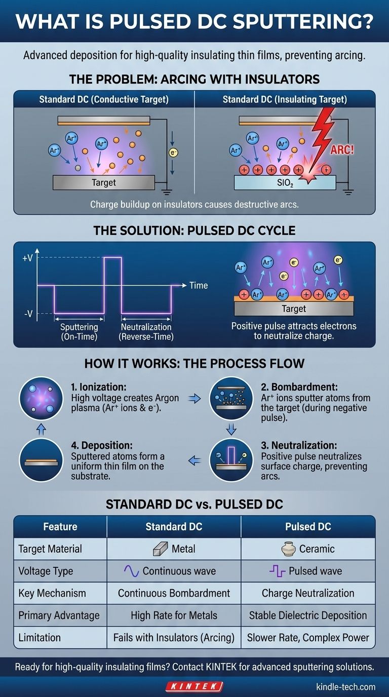
In essence, pulsed DC sputtering is an advanced deposition technique that applies a DC voltage in short, controlled pulses rather than continuously. This method is specifically designed to deposit high-quality thin films of insulating or "dielectric" materials, such as oxides and nitrides, by preventing a catastrophic electrical issue known as arcing that plagues standard DC sputtering in these applications.
The core problem with standard DC sputtering is that it works beautifully for conductive metals but fails when used with insulating materials. Pulsed DC sputtering solves this by periodically reversing the electrical charge on the target, neutralizing a charge buildup that would otherwise lead to destructive arcing.
The Foundation: Understanding Standard Sputtering
To understand why pulsed DC is necessary, we must first understand the standard sputtering process. It is a physical vapor deposition (PVD) method that occurs inside a vacuum chamber.
The Sputtering Environment
The process begins by placing a substrate (the object to be coated) and a target (the material to be deposited) into a vacuum chamber. The chamber is pumped down to a very low pressure and then backfilled with a small, controlled amount of an inert gas, most commonly Argon (Ar).
Creating the Plasma
A strong negative DC voltage is applied to the target material. This high voltage ionizes the surrounding Argon gas, stripping electrons from the Argon atoms and creating a mixture of positively charged Argon ions (Ar+) and free electrons known as a plasma.
The Bombardment Process
The positively charged Argon ions are powerfully accelerated toward the negatively charged target. They collide with the target surface with immense force, transferring their momentum and knocking loose, or "sputtering," individual atoms of the target material.
Film Deposition
These sputtered atoms travel through the vacuum chamber and land on the substrate, gradually building up, atom by atom, to form a dense and uniform thin film.
The Critical Limitation: Sputtering Insulating Materials
The standard DC sputtering process described above has a fundamental weakness that makes it unsuitable for a large class of important materials.
The "Arcing" Problem
When the target material is a conductor (like titanium or aluminum), the positive charge from the impacting Argon ions is immediately conducted away.
However, if the target is an electrical insulator (like silicon dioxide or aluminum oxide), it cannot conduct electricity. The positive charge from the Argon ions accumulates on the target's surface, a phenomenon called "target poisoning."
When this positive charge builds to an extreme level, it will suddenly and violently discharge to a nearby grounded surface in the chamber. This event is an arc, a miniature lightning strike that can damage or destroy the target, contaminate the chamber, and ruin the film being deposited.
The Solution: How Pulsed DC Works
Pulsed DC sputtering was developed specifically to solve the problem of arcing when depositing insulating films.
Introducing the Pulse
Instead of a constant negative voltage, a specialized power supply applies the voltage in rapid pulses. A typical cycle involves a long period of negative voltage (the "on-time") followed by a very brief period of positive voltage (the "reverse-time" or "off-time").
Neutralizing Charge Buildup
During the main negative pulse, sputtering occurs just as it does in the standard DC process.
Crucially, during the brief positive reversal, the target becomes positively charged. This attracts the highly mobile electrons from the plasma, which flood the target surface and neutralize the positive ion charge that had accumulated during the sputtering phase.
Preventing Arcs for Stable Deposition
This cycle repeats thousands of times per second. By constantly neutralizing the surface charge before it can build up to a critical level, pulsed DC effectively prevents arcing. This allows for the stable, long-term deposition of high-quality dielectric films without process interruptions or damage.
Understanding the Trade-offs
While it is a powerful solution, pulsed DC sputtering is not without its considerations.
Slower Deposition Rates
Because the target is not being sputtered during the brief positive pulse, the overall deposition rate is slightly lower than what would be theoretically possible with continuous DC sputtering on a conductive target.
Power Supply Complexity
Pulsed DC power supplies are significantly more complex and expensive than their simple, continuous DC counterparts. They require precise control over pulse frequency, duty cycle, and reverse voltage.
Added Process Variables
The pulse frequency and duration become additional parameters that must be carefully optimized. Finding the right balance is key to maximizing the deposition rate while completely suppressing any arcing events.
Making the Right Choice for Your Goal
Selecting a sputtering method depends entirely on the material you intend to deposit.
- If your primary focus is depositing conductive materials (like metals): Standard DC magnetron sputtering is almost always the most efficient, fastest, and most cost-effective choice.
- If your primary focus is depositing insulating or semiconductive materials (like oxides, nitrides, or ceramics): Pulsed DC sputtering is the industry-standard solution for achieving a stable process and high-quality films at industrial scales.
- If your primary focus is depositing any type of material with maximum versatility in a research setting: RF (Radio Frequency) sputtering is the classic alternative for insulating targets, though it typically involves more complex impedance matching and often has lower deposition rates than pulsed DC.
Ultimately, choosing the right deposition technique is about matching the tool to the specific electrical properties of your target material.
Summary Table:
| Feature | Standard DC Sputtering | Pulsed DC Sputtering |
|---|---|---|
| Target Material | Conductive metals (e.g., Ti, Al) | Insulating/dielectric materials (e.g., SiO₂, Al₂O₃) |
| Voltage Type | Continuous negative DC | Pulsed negative/positive DC |
| Key Mechanism | Continuous ion bombardment | Charge neutralization during positive pulse |
| Primary Advantage | High deposition rate for metals | Prevents arcing, enables stable dielectric deposition |
| Limitation | Fails with insulators (causes arcing) | Slower deposition rate, more complex power supply |
Ready to deposit high-quality insulating films without arcing?
Pulsed DC sputtering is essential for stable, industrial-scale deposition of dielectric materials like oxides and nitrides. At KINTEK, we specialize in advanced lab equipment, including sputtering systems tailored to your specific research and production needs.
Our experts can help you select the right PVD solution to enhance your thin film processes. Contact us today to discuss how KINTEK's reliable sputtering technology can advance your laboratory's capabilities!
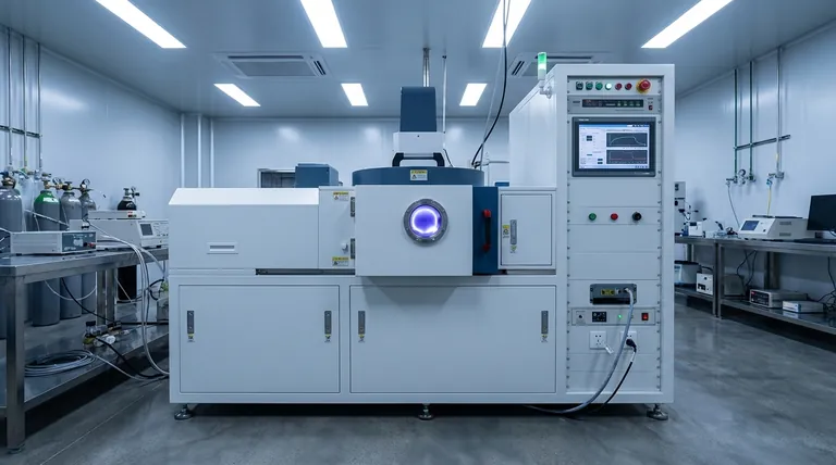
Visual Guide
Related Products
- Spark Plasma Sintering Furnace SPS Furnace
- Chemical Vapor Deposition CVD Equipment System Chamber Slide PECVD Tube Furnace with Liquid Gasifier PECVD Machine
People Also Ask
- What is the difference between spark plasma sintering and flash sintering? A Guide to Advanced Sintering Methods
- What is the theory of spark plasma sintering? A Guide to Rapid, Low-Temperature Densification
- What are the fundamentals of spark plasma sintering process? Unlock Rapid, High-Performance Material Consolidation
- What is the mechanism of SPS process? A Deep Dive into Rapid, Low-Temperature Sintering
- What is the pressure for spark plasma sintering? A Guide to Optimizing SPS Parameters

