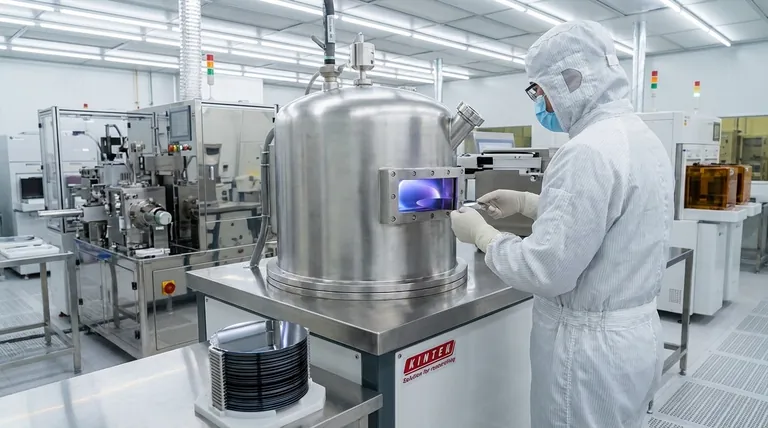
In semiconductor manufacturing, Physical Vapor Deposition (PVD) is a high-precision process used to apply extremely thin, pure films of materials onto a substrate, most commonly a silicon wafer. This technique is not merely a coating; it is a fundamental step in building the microscopic metal layers that form the intricate wiring and conductive pathways inside a microchip.
The core function of PVD in the semiconductor industry is to enable the creation of reliable, high-performance microelectronics. Its value comes from its ability to deposit materials with the exceptional purity and structural uniformity that modern chips demand, a level of precision that older methods cannot achieve.
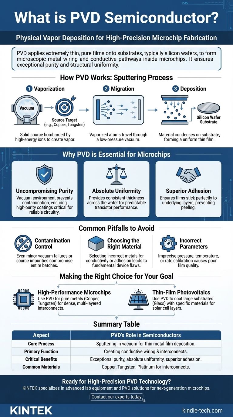
How PVD Works in a Semiconductor Context
PVD is a vacuum deposition process, meaning it occurs in a low-pressure environment to prevent contamination. The process, often a specific type called sputtering, universally involves three core stages.
Step 1: Vaporization
First, a solid source material (known as a "target") is converted into a vapor. This is typically done by bombarding the target—which could be a metal like copper, tungsten, or platinum—with high-energy ions inside the vacuum chamber.
Step 2: Migration
The vaporized atoms or molecules travel through the vacuum chamber from the source target toward the substrate. The vacuum ensures their path is unobstructed by air or other unwanted particles.
Step 3: Deposition
Finally, the vaporized material lands and condenses on the surface of the semiconductor wafer, forming a thin, solid film. This film can be a single layer or one of many layers built up to create complex circuits.
Why PVD is Essential for Microchip Fabrication
The unique characteristics of PVD films are what make the technology indispensable for creating reliable and powerful semiconductors. The performance of a modern microchip is directly tied to the quality of these deposited layers.
Uncompromising Purity
Semiconductor circuitry is exquisitely sensitive to contamination. PVD's vacuum environment and process control yield coatings of exceptionally high purity, preventing unwanted chemical reactions or electrical failures in the final chip.
Absolute Uniformity
PVD creates films with excellent thickness uniformity across the entire wafer. This consistency is critical for ensuring that every one of the millions or billions of transistors on a chip behaves predictably.
Superior Adhesion
The deposited metal films must stick perfectly to the underlying layers of the wafer. PVD provides excellent adhesion, preventing layers from peeling or delaminating during subsequent manufacturing steps or device operation.
Common Pitfalls to Avoid
While PVD is a cornerstone technology, its success depends on meticulous control over the process parameters. Overlooking these details can lead to device failure.
Contamination Control is Paramount
The entire value of PVD lies in its purity. Any failure in the vacuum system or contamination of the source material will compromise the entire batch of wafers, rendering the resulting chips useless.
Choosing the Right Material
Not all materials are suited for every application. Using a metal with poor conductivity for an interconnect layer or one with poor adhesion on a specific substrate will create a fundamental flaw in the device's architecture.
Incorrect Deposition Parameters
Factors like pressure, temperature, and deposition rate must be precisely calibrated. A rate that is too fast can lead to a rough, poorly adhered film, while one that is too slow can be economically unviable and introduce thermal stress.
Making the Right Choice for Your Goal
The application of PVD technology is tailored to the desired outcome of the electronic device.
- If your primary focus is high-performance microchips: PVD is used to deposit pure metals like copper or tungsten, which form the dense, multi-layered interconnects that allow electrical signals to travel quickly and reliably between transistors.
- If your primary focus is thin-film photovoltaics: PVD is the method for coating large substrates like glass with specific materials such as copper, indium, or gallium to create the active layers of a solar cell.
Ultimately, PVD is a foundational enabling technology, providing the atomic-level precision required to build the complex structures that power our digital world.
Summary Table:
| Key Aspect | PVD's Role in Semiconductors |
|---|---|
| Core Process | Sputtering in a vacuum to deposit thin metal films on wafers. |
| Primary Function | Creating the conductive wiring and interconnects within a microchip. |
| Critical Benefits | Exceptional purity, absolute film uniformity, and superior adhesion. |
| Common Materials | Copper, Tungsten, Platinum for interconnects and conductive layers. |
Ready to integrate high-precision PVD technology into your semiconductor fabrication process?
KINTEK specializes in advanced lab equipment and consumables, providing the reliable PVD solutions your laboratory needs to achieve the exceptional film purity and uniformity required for next-generation microchips. Our expertise supports the entire semiconductor manufacturing workflow.
Contact our experts today to discuss how our PVD systems can enhance your chip performance and yield.
Visual Guide
Related Products
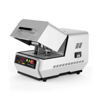
- HFCVD Machine System Equipment for Drawing Die Nano-Diamond Coating
- 915MHz MPCVD Diamond Machine Microwave Plasma Chemical Vapor Deposition System Reactor
- Custom PTFE Wafer Holders for Lab and Semiconductor Processing
- Vacuum Hot Press Furnace Machine for Lamination and Heating
- Anti-Cracking Press Mold for Lab Use
People Also Ask
- How do CVD diamonds grow? A Step-by-Step Guide to Lab-Grown Diamond Creation
- How is something diamond coated? A Guide to CVD Growth vs. Plating Methods
- What is direct current DC magnetron sputtering? A Guide to High-Quality Thin Film Deposition
- What is the process of coating deposition? A Step-by-Step Guide to Thin Film Engineering
- Is sputtering a PVD? Discover the Key Coating Technology for Your Lab