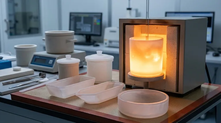
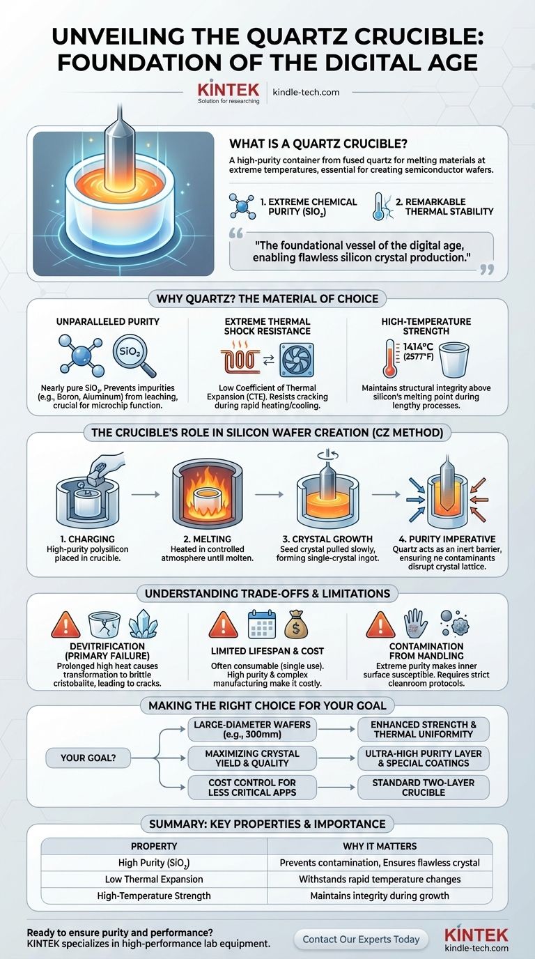
At its core, a quartz crucible is a high-purity container engineered from fused quartz, designed to hold and melt materials at extreme temperatures. It is an indispensable tool in high-tech manufacturing, most notably for melting the polysilicon used to grow the single-crystal silicon ingots that become semiconductor wafers.
The quartz crucible is the foundational vessel of the digital age. Its two essential properties—extreme chemical purity and remarkable thermal stability—are what make it possible to produce the flawless silicon crystals required for virtually all modern electronics.
Why Quartz Is the Material of Choice
The selection of fused quartz is not accidental; its unique properties are critical for the demanding environments where these crucibles are used. No other commercially viable material combines these characteristics as effectively.
Unparalleled Purity
A quartz crucible is made from high-purity quartz sand, resulting in a container that is essentially pure silicon dioxide (SiO₂). This is crucial because when melting silicon, any impurities from the container (like boron or aluminum) can leach into the melt, altering its electrical properties and rendering the final microchips useless.
Extreme Thermal Shock Resistance
Fused quartz has an exceptionally low coefficient of thermal expansion (CTE). This means it expands and contracts very little when subjected to rapid and extreme temperature changes. This stability prevents the crucible from cracking during the heating and cooling cycles of the silicon melting process.
High-Temperature Strength
The crucible must maintain its structural integrity well above the melting point of silicon, which is approximately 1414°C (2577°F). Fused quartz can withstand these temperatures, providing a stable container for the molten silicon throughout the lengthy crystal growth process.
The Crucible's Role in Creating Silicon Wafers
The primary application for quartz crucibles is the Czochralski (CZ) method, the dominant process for producing single-crystal silicon for the semiconductor industry.
The Czochralski (CZ) Process
In this method, high-purity, solid polysilicon is placed into the quartz crucible. The crucible is then heated in a controlled atmosphere furnace until the silicon melts.
From Molten Silicon to Crystal Ingot
Once the silicon is molten, a small "seed crystal" is lowered into the melt and then slowly pulled upwards while rotating. As it is pulled, the molten silicon solidifies onto the seed, inheriting its perfect crystal structure and forming a large, cylindrical single-crystal ingot.
The Purity Imperative
This entire process relies on maintaining the absolute purity of the molten silicon. The quartz crucible acts as an inert barrier, ensuring that no contaminants are introduced that could disrupt the crystal lattice or degrade the performance of the final integrated circuits.
Understanding the Trade-offs and Limitations
While essential, quartz crucibles are not without their challenges. Understanding their limitations is key to managing yield and quality in manufacturing.
Devitrification: The Primary Failure Mode
The most significant limitation is devitrification. At prolonged high temperatures, the amorphous (non-crystalline) structure of the fused quartz begins to transform into a crystalline state called cristobalite. This new structure is brittle and has a different CTE, creating stress that can cause the crucible to crack, potentially leading to catastrophic failure and loss of the entire silicon melt.
Limited Lifespan and Cost
Due to the stresses of the CZ process and the risk of devitrification, high-purity quartz crucibles are often considered consumable items, sometimes used for only a single crystal growth cycle. Their high purity and complex manufacturing process make them a significant operational cost.
Contamination from Handling
The extreme purity of the crucible's inner surface makes it highly susceptible to contamination. Even fingerprints can introduce impurities like sodium or potassium. This necessitates strict handling protocols and cleanroom environments throughout the crucible's lifecycle.
Making the Right Choice for Your Goal
Selecting a crucible involves balancing performance, lifespan, and cost based on the specific manufacturing objective.
- If your primary focus is producing large-diameter wafers (e.g., 300mm): You need crucibles with enhanced mechanical strength and thermal uniformity to manage the massive volume and weight of the silicon melt.
- If your primary focus is maximizing crystal yield and quality: Prioritize crucibles with an ultra-high purity inner layer and specialized coatings designed to suppress devitrification, extending stable melt times.
- If your primary focus is cost control for less critical applications: A standard two-layer crucible without advanced coatings might provide the necessary performance at a lower cost per unit.
Ultimately, the quartz crucible is a piece of precision-engineered equipment whose performance is directly linked to the quality and efficiency of advanced manufacturing processes.
Summary Table:
| Property | Why It Matters for Semiconductor Manufacturing |
|---|---|
| High Purity (SiO₂) | Prevents contamination of the silicon melt, ensuring flawless crystal structure for microchips. |
| Low Thermal Expansion | Withstands rapid temperature changes (heating/cooling cycles) without cracking. |
| High-Temperature Strength | Maintains integrity above silicon's melting point (1414°C/2577°F) during crystal growth. |
Ready to ensure the purity and performance of your high-temperature processes?
KINTEK specializes in high-performance lab equipment and consumables, including precision crucibles designed for demanding applications. Our expertise supports laboratories in semiconductor research, materials science, and advanced manufacturing.
Contact our experts today to discuss how the right equipment can enhance your yield, quality, and efficiency.
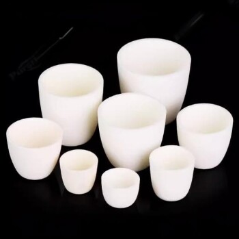
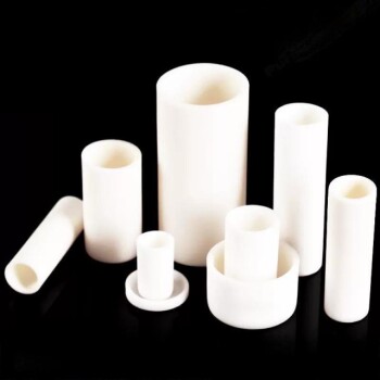
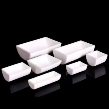
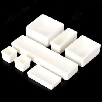
Visual Guide
Related Products
- High Purity Pure Graphite Crucible for Evaporation
- Electron Beam Evaporation Coating Tungsten Crucible and Molybdenum Crucible for High Temperature Applications
- Electron Beam Evaporation Coating Gold Plating Tungsten Molybdenum Crucible for Evaporation
- Arc-Shaped Alumina Ceramic Crucible High Temperature Resistant for Engineering Advanced Fine Ceramics
- Electron Beam Evaporation Coating Oxygen-Free Copper Crucible and Evaporation Boat
People Also Ask
- What are the advantages of using graphite crucibles in 3000°C experiments? Achieve Superior Purity and Performance
- Why is a high-purity graphite crucible ideal for nitrogen-doped graphene at 1500 °C? Maximize Purity and Stability
- Why must high-purity graphite crucibles be treated in a vacuum oven and pre-baked? Ensure Pure Molten Salt Experiments
- Why are high-purity graphite crucibles preferred for sulfide solid electrolytes? Achieve Superior Material Purity
- What role does a high-purity graphite crucible play in CaO-MgO-Al2O3-SiO2 system equilibrium experiments? Maximize Accuracy