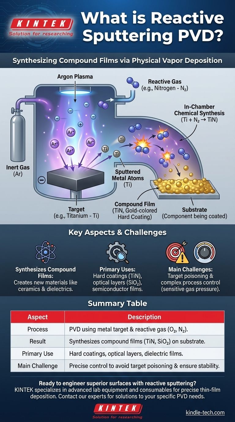
Reactive sputtering is a physical vapor deposition (PVD) technique used to create thin compound films. It builds upon standard sputtering by introducing a reactive gas, like oxygen or nitrogen, into the vacuum chamber along with an inert gas like argon. As atoms are ejected from a metal target, they chemically react with this gas to form a new compound material, such as an oxide or nitride, which is then deposited onto the substrate.
The essential purpose of reactive sputtering is not to simply deposit the target material, but to synthesize a completely new compound film during the deposition process. It transforms a pure metal target into a high-performance ceramic, dielectric, or semiconductor layer on a component's surface.
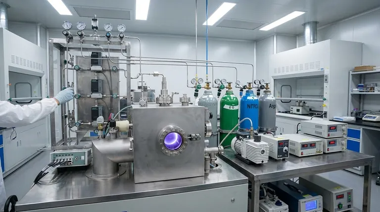
The Mechanics of Sputtering: A Foundation
To understand the "reactive" component, we must first establish the fundamentals of the standard sputtering process. This method is valued for creating extremely uniform, high-quality thin films.
The Plasma Environment
The process begins by introducing a small amount of an inert gas, most commonly argon, into a vacuum chamber. A high voltage is applied, which strips electrons from the argon atoms and creates a plasma—a superheated, ionized gas containing positive argon ions and free electrons.
Target Bombardment
A component made of the desired coating material, known as the target, is given a negative electrical charge. The positively charged argon ions in the plasma are aggressively pulled toward this negative target, striking its surface with significant energy.
Material Deposition
This high-energy ion bombardment acts like a microscopic sandblaster, dislodging or "sputtering" individual atoms from the target material. These liberated atoms travel through the chamber and deposit onto the substrate (the part being coated), gradually building a thin, uniform film.
Introducing the "Reactive" Element
Reactive sputtering introduces a critical second step into this process, fundamentally changing the nature of the deposited film.
Adding a Second Gas
Alongside the inert argon gas, a carefully controlled amount of a reactive gas is introduced into the chamber. The choice of gas depends on the desired final compound. Common examples include oxygen (to form oxides), nitrogen (to form nitrides), or methane (to form carbides).
In-Chamber Chemical Synthesis
As the metal atoms are sputtered from the target, they travel through the plasma environment, which is now rich with this reactive gas. During this transit, the metal atoms chemically bond with the reactive gas particles.
Forming a New Compound Film
The material that ultimately deposits on the substrate is not the pure metal from the target but a completely new compound. For example:
- Sputtering a titanium target in a nitrogen atmosphere creates a hard, gold-colored titanium nitride (TiN) film.
- Sputtering a silicon target in an oxygen atmosphere creates a clear, insulating silicon dioxide (SiO₂) film.
This allows for the creation of materials like ceramics and dielectrics that would be difficult or impossible to use as a sputter target directly.
Understanding the Trade-offs and Challenges
While powerful, reactive sputtering introduces complexities that require careful management to achieve consistent, high-quality results.
Target Poisoning
The primary challenge is "target poisoning." This occurs when the reactive gas reacts not only with the sputtered atoms but also with the surface of the target itself. This forms an insulating compound layer on the target, which drastically reduces the sputtering rate and can make the process unstable.
Process Control Complexity
The deposition rate and film properties are highly sensitive to the partial pressure of the reactive gas. Maintaining the delicate balance between having enough reactive gas to form the desired compound without poisoning the target requires sophisticated process control systems, including feedback loops and gas flow controllers.
When to Choose Reactive Sputtering
The decision to use reactive sputtering is determined by the specific properties required in the final thin film.
- If your primary focus is creating hard, wear-resistant ceramic coatings: Reactive sputtering is the ideal method for depositing materials like titanium nitride (TiN) or aluminum nitride (AlN) for tools and industrial components.
- If your primary focus is depositing high-quality optical or dielectric films: The process excels at creating compounds like silicon dioxide (SiO₂) and tantalum nitride (TaN) for anti-reflective coatings, semiconductor circuits, and thin-film resistors.
- If your primary focus is depositing a pure metal or alloy with no chemical changes: Standard, non-reactive sputtering using only an inert gas is the correct and more straightforward choice.
By enabling the synthesis of new materials during deposition, reactive sputtering provides a precise and powerful tool for engineering advanced surfaces.
Summary Table:
| Key Aspect | Description |
|---|---|
| Process | PVD technique using a metal target & reactive gas (e.g., O₂, N₂). |
| Result | Synthesizes compound films (e.g., TiN, SiO₂) on the substrate. |
| Primary Use | Hard coatings, optical layers, dielectric films for semiconductors. |
| Main Challenge | Requires precise control to avoid target poisoning and ensure stability. |
Ready to engineer superior surfaces with reactive sputtering?
KINTEK specializes in advanced lab equipment and consumables for precise thin-film deposition. Whether you're developing wear-resistant tool coatings, optical layers, or semiconductor components, our expertise ensures you achieve consistent, high-quality results.
Contact our experts today to discuss how our solutions can meet your laboratory's specific PVD needs.
Visual Guide
Related Products
- Inclined Rotary Plasma Enhanced Chemical Vapor Deposition PECVD Equipment Tube Furnace Machine
- HFCVD Machine System Equipment for Drawing Die Nano-Diamond Coating
- Vacuum Hot Press Furnace Machine for Lamination and Heating
- 915MHz MPCVD Diamond Machine Microwave Plasma Chemical Vapor Deposition System Reactor
- Customer Made Versatile CVD Tube Furnace Chemical Vapor Deposition Chamber System Equipment
People Also Ask
- What is PECVD silicon deposition? Achieve Low-Temperature, High-Quality Thin Films
- What is PECVD used for? Achieve Low-Temperature, High-Performance Thin Films
- What is plasma in CVD process? Lowering Deposition Temperatures for Heat-Sensitive Materials
- What is the difference between PECVD and CVD? Unlock the Right Thin-Film Deposition Method
- How does plasma enhanced CVD work? Achieve Low-Temperature, High-Quality Thin Film Deposition


