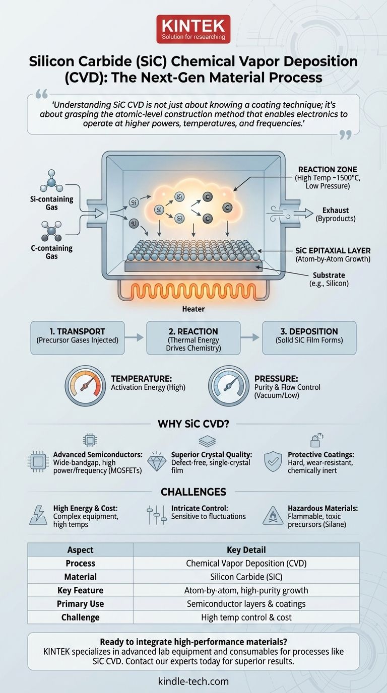
In essence, Silicon Carbide (SiC) Chemical Vapor Deposition (CVD) is a highly controlled manufacturing process used to grow crystalline films of silicon carbide onto a substrate. It involves introducing reactive gases containing silicon and carbon into a chamber, where high temperatures cause them to react and deposit a solid, high-purity SiC layer atom by atom on a target surface. This method is fundamental to producing the next generation of high-performance semiconductor devices.
Understanding SiC CVD is not just about knowing a coating technique; it's about grasping the atomic-level construction method that enables electronics to operate at higher powers, temperatures, and frequencies than is possible with traditional silicon.
How Chemical Vapor Deposition Fundamentally Works
The power of CVD lies in its ability to build materials from the ground up, starting with gas molecules. The process provides an exceptional level of control over the final material's purity and structure.
The Core Principle: Gas to Solid
At its heart, CVD is a process that converts volatile precursor gases into a stable solid film. A workpiece, or substrate, is placed inside a reaction chamber under tightly controlled conditions.
The chamber is then filled with specific gases. These gases are not the final material but are chemical compounds that contain the atoms needed for the final film—in this case, silicon and carbon.
The Three-Step Process
The deposition process can be broken down into three key stages:
- Transport: Volatile precursor gases, such as a silicon source (e.g., silane, SiH₄) and a carbon source (e.g., propane, C₃H₈), are precisely injected into the reaction chamber.
- Reaction: The substrate is heated to very high temperatures (often over 1500°C for SiC). This thermal energy breaks down the precursor gases and drives chemical reactions on the hot substrate surface.
- Deposition: The non-volatile product of the reaction—solid silicon carbide—deposits onto the substrate, forming a thin, uniform, and often single-crystal film. Excess gaseous byproducts are pumped out of the chamber.
The Critical Role of Temperature and Pressure
Achieving a high-quality SiC film is impossible without precise environmental control. Temperature provides the activation energy needed for the chemical reactions to occur.
Pressure, which is often held at a vacuum or near-vacuum level, is just as critical. It ensures the purity of the environment, prevents unwanted reactions, and helps control the flow of the reactive gases toward the substrate surface for uniform deposition.
Why SiC is a Prime Candidate for CVD
While CVD is used for many materials, its pairing with silicon carbide is driving a revolution in power electronics and other demanding fields.
Creating Advanced Semiconductors
Traditional silicon struggles in high-power, high-frequency, and high-temperature applications. SiC is a wide-bandgap semiconductor, meaning it can withstand much higher voltages and temperatures before breaking down.
CVD is the premier method for growing the ultra-pure, defect-free epitaxial layers of SiC that are required to manufacture robust and efficient power devices like MOSFETs and Schottky diodes.
Ensuring Superior Crystal Quality
The performance of a semiconductor device is directly tied to the perfection of its crystal lattice. The slow, controlled, layer-by-layer growth enabled by CVD is essential for creating this perfection.
This level of precision minimizes defects that would otherwise trap charge and degrade the electronic performance of the final device, which is why the process requires a high degree of technical skill to master.
Applications in Protective Coatings
Beyond electronics, SiC is incredibly hard, chemically inert, and wear-resistant. Using CVD, a thin but durable layer of SiC can be applied to industrial components like cutting tools, bearings, or pump seals to dramatically extend their operational lifetime.
Understanding the Trade-offs and Challenges
While powerful, SiC CVD is not a simple or inexpensive process. It comes with significant engineering and operational challenges.
High Energy and Equipment Costs
The extremely high temperatures required to grow quality SiC crystals mean the process is very energy-intensive. The reactors themselves must be built from specialized materials that can withstand these harsh conditions, making the equipment complex and expensive.
Intricate Process Control
Success hinges on meticulous control. Tiny fluctuations in temperature, pressure, or gas flow rates can introduce defects into the crystal structure, rendering the final wafer useless. Maintaining uniformity across a large substrate is a major engineering hurdle.
Hazardous Precursor Materials
The precursor gases used in the process, such as silane, can be highly flammable and toxic. Safely handling, storing, and delivering these materials requires stringent safety protocols and specialized infrastructure.
How to Apply This to Your Project
Your choice to use or specify SiC CVD depends entirely on the performance requirements of your end product.
- If your primary focus is high-performance power electronics: CVD is the essential, non-negotiable process for growing the active epitaxial layers needed for SiC MOSFETs, diodes, and other power-switching devices.
- If your primary focus is producing bulk SiC wafers (substrates): A related high-temperature process called Physical Vapor Transport (PVT) is typically used for creating the initial bulk crystal ingot, but CVD is then used to grow the critical device layers on top of the sliced wafers.
- If your primary focus is creating extremely hard, wear-resistant coatings: CVD is an excellent choice for depositing a thin, uniform, and highly adherent SiC film on components that operate in harsh mechanical or chemical environments.
Ultimately, SiC CVD is the key enabling technology that unlocks the superior properties of silicon carbide for demanding real-world applications.
Summary Table:
| Aspect | Key Detail |
|---|---|
| Process Type | Chemical Vapor Deposition (CVD) |
| Material | Silicon Carbide (SiC) |
| Key Feature | Atom-by-atom, high-purity crystalline film growth |
| Primary Use | Semiconductor epitaxial layers & protective coatings |
| Main Challenge | High-temperature process control & high cost |
Ready to integrate high-performance materials into your lab's workflow? KINTEK specializes in providing the advanced lab equipment and consumables needed for cutting-edge processes like SiC CVD. Whether you are developing next-generation semiconductors or require durable coatings for industrial components, our expertise supports your innovation. Contact our experts today to discuss how we can help you achieve superior results.
Visual Guide
Related Products
- Customer Made Versatile CVD Tube Furnace Chemical Vapor Deposition Chamber System Equipment
- Custom CVD Diamond Coating for Lab Applications
- CVD Diamond Wire Drawing Die Blanks for Precision Applications
- CVD Diamond Cutting Tool Blanks for Precision Machining
- CVD Diamond Dressing Tools for Precision Applications
People Also Ask
- What is the synthesis and mechanism involved in the preparation of carbon nanotubes using CVD process? Master Controlled Growth for Your Application
- What is the function of a tube furnace in CVD SiC synthesis? Achieving Ultra-Pure Silicon Carbide Powders
- What is a CVD tube furnace? A Complete Guide to Thin-Film Deposition
- How does a CVD tube furnace inhibit the sintering of silver supports? Boost Membrane Durability and Performance
- What method is used to grow graphene? Master High-Quality Production with CVD