In Scanning Electron Microscopy (SEM), sputter coating is a fundamental sample preparation technique used to apply an ultra-thin, electrically conductive layer of metal onto a non-conductive or poorly conductive specimen. This process is essential for preventing a build-up of static charge from the microscope's electron beam, which would otherwise severely distort the image. By making the sample's surface conductive, sputter coating dramatically improves image quality, resolution, and stability.
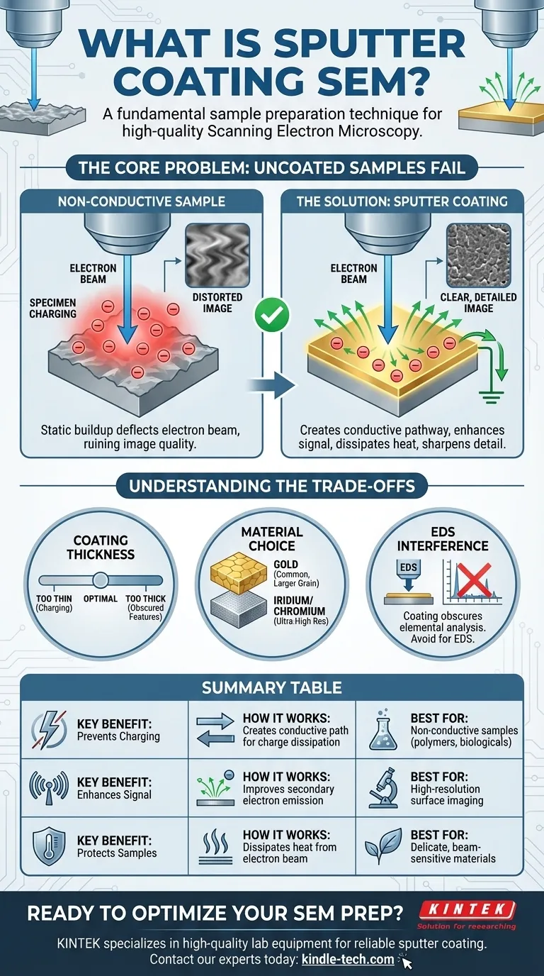
The core problem with non-conductive SEM samples is that the electron beam creates a static charge build-up, which deflects electrons and ruins the image. Sputter coating solves this by creating a conductive pathway for that charge to dissipate, enabling clear and detailed surface analysis.
The Core Problem: Why Uncoated Samples Fail
In SEM, an image is formed by detecting electrons that are emitted from a sample's surface when it's hit by a high-energy electron beam. This process runs into a fundamental problem with materials that don't conduct electricity.
The Issue of "Specimen Charging"
When the electron beam strikes a non-conductive surface, the electrons from the beam accumulate on that spot. Because the material cannot conduct this excess charge away, a localized negative static field builds up on the sample.
How Charging Distorts the Image
This static charge wreaks havoc on the imaging process. It can deflect the incoming primary electron beam, causing the image to drift or become distorted. It also disrupts the path of the emitted secondary electrons, leading to bright patches, streaks, and a complete loss of topographical detail.
The Impact on Signal Detection
A negatively charged surface actively repels the low-energy secondary electrons that the detector needs to form a high-resolution image. This leads to a very poor signal-to-noise ratio, resulting in a noisy or featureless image.
How Sputter Coating Provides the Solution
Sputter coating directly neutralizes the problem of specimen charging while adding several other key benefits for high-quality imaging. The process typically applies a metal film between 2 and 20 nanometers thick.
Creating a Conductive Pathway
The thin layer of metal (often gold, platinum, or iridium) acts as a perfect electrical conductor. It provides a path for any excess electrons from the beam to travel harmlessly away to the grounded sample holder, preventing any charge from building up.
Enhancing Secondary Electron Emission
The heavy metals used for coating are excellent emitters of secondary electrons. When the primary beam interacts with this highly emissive layer, it generates a much stronger, clearer signal for the detector. This dramatically improves the signal-to-noise ratio.
Improving Thermal Conduction
The electron beam also deposits a significant amount of heat onto the sample. The metal coating helps dissipate this thermal energy, protecting delicate specimens like polymers or biological samples from being damaged or melted by the beam.
Sharpening Surface Detail
The dense metal coating reduces how far the electron beam penetrates into the sample. This ensures that the detected signal originates from the absolute top surface, which significantly improves the resolution of fine surface features and sharpens the appearance of edges.
Understanding the Trade-offs
While essential, sputter coating is a process that must be managed carefully. The goal is to solve the charging problem without introducing new artifacts.
Coating Thickness is Critical
There is a fine balance to strike with coating thickness. If the layer is too thin, charging may still occur. If it is too thick, the coating can obscure the true nano-scale features of the specimen's original surface.
Material Choice Matters
Different coating metals have different grain sizes. Gold is common and effective, but its relatively large grain structure can become visible at very high magnifications. For ultra-high resolution work, finer-grained metals like chromium or iridium are superior choices.
It Can Obscure Elemental Analysis
Sputter coating is ideal for imaging surface topography. However, if your goal is to determine the elemental composition of your sample using Energy-Dispersive X-ray Spectroscopy (EDS), the metal coating will interfere. The EDS detector will primarily see the coating material (e.g., gold) instead of the elements in the underlying sample.
Making the Right Choice for Your Goal
Sputter coating is not a one-size-fits-all solution. Your analytical goal should dictate your sample preparation strategy.
- If your primary focus is high-resolution surface imaging: Sputter coating is almost always required for non-conductive samples to prevent charging and enhance signal quality.
- If your primary focus is determining elemental composition (EDS): You must avoid sputter coating with metal. Consider using a carbon coater or analyzing the sample uncoated at a very low beam voltage.
- If you are working with extremely delicate, beam-sensitive samples: A conductive coating provides crucial thermal and physical protection, but you must carefully control the thickness to preserve the original surface features.
Ultimately, sputter coating is a foundational tool that transforms challenging, non-conductive materials into ideal subjects for high-quality SEM analysis.
Summary Table:
| Key Benefit | How It Works | Best For |
|---|---|---|
| Prevents Charging | Creates a conductive path to dissipate static charge. | Non-conductive samples like polymers and biologicals. |
| Enhances Signal | Improves secondary electron emission for a clearer image. | High-resolution surface topography imaging. |
| Protects Samples | Dissipates heat from the electron beam. | Delicate, beam-sensitive materials. |
Ready to optimize your SEM sample preparation?
KINTEK specializes in high-quality lab equipment and consumables for reliable and precise sputter coating. Our solutions are designed to meet the demanding needs of laboratory professionals, ensuring you achieve the highest quality imaging results without specimen charging or damage.
Contact our experts today to discuss how our sputter coaters and consumables can enhance your SEM analysis workflow and deliver the clarity and detail your research demands.
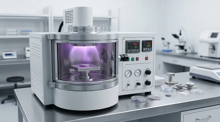
Visual Guide
Related Products
People Also Ask
- How can we create a reducing environment? Master the Methods for Precise Chemical Control
- Why do we need optical coating? To Control Light and Enhance Optical Performance
- What is the optical coating? Master Light Control for Superior Optical Performance
- Is Sputter Tint good? Premium Heat Rejection & Long-Term Durability Explained
- What is the thinnest coating? Unlocking Unique Properties at the Atomic Scale
