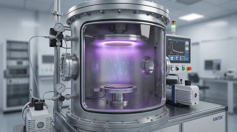
In essence, sputtering is a physical vapor deposition (PVD) process used to create exceptionally thin and uniform films of material onto a surface, known as a substrate. It operates by ejecting atoms from a source material (the "target") by bombarding it with energized ions inside a vacuum. These ejected atoms then travel and condense onto the substrate, building the desired coating one atomic layer at a time.
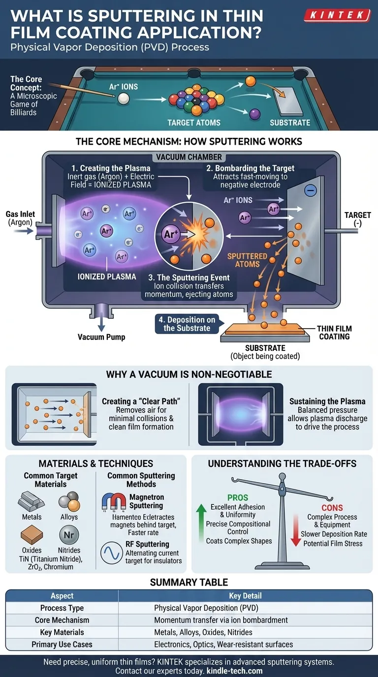
Sputtering is not a chemical reaction or a simple spray-on technique; it is a momentum transfer process. Think of it as a microscopic game of billiards where high-energy ions are the cue balls, knocking atoms loose from a target so they can deposit elsewhere to form a high-performance film.
The Core Mechanism: How Sputtering Works
Sputtering is a highly controlled process that takes place within a sealed vacuum chamber. The entire mechanism can be broken down into a few fundamental steps.
Step 1: Creating the Plasma
The process begins by introducing a small amount of an inert gas, typically Argon, into the vacuum chamber. An electric field is then applied, which energizes the gas and strips electrons from the Argon atoms, creating a glowing, ionized gas known as a plasma. This plasma consists of positively charged Argon ions and free electrons.
Step 2: Bombarding the Target
The source material to be deposited, called the target, is given a strong negative electrical charge. This negative charge powerfully attracts the positively charged ions from the plasma, causing them to accelerate and collide with the target's surface at high speed.
Step 3: The Sputtering Event
When these high-energy ions strike the target, they transfer their momentum to the atoms on the target's surface. If the energy is sufficient, this collision ejects or "sputters" atoms from the target material, sending them out into the vacuum chamber.
Step 4: Deposition on the Substrate
These sputtered atoms travel through the vacuum until they reach the substrate (the object being coated). Upon arrival, they condense onto its surface, gradually building a thin, dense, and highly uniform film.
Why a Vacuum is Non-Negotiable
The entire sputtering process relies on maintaining a carefully controlled vacuum environment for two critical reasons.
Creating a "Clear Path"
A vacuum removes air and other particles from the chamber. This ensures that the sputtered atoms can travel from the target to the substrate with minimal collisions or resistance. Without a vacuum, the sputtered atoms would collide with air molecules, scattering them and preventing the formation of a clean, dense film.
Sustaining the Plasma
While a deep vacuum is needed, a small amount of gas is required to create the plasma. The pressure must be perfectly balanced—low enough to allow for a clear path, but high enough to sustain the plasma discharge that drives the entire process.
Materials and Techniques
Sputtering is valued for its versatility, capable of depositing a vast range of materials using several refined methods.
Common Target Materials
The process is not limited to pure metals. It is frequently used to deposit alloys, oxides, and nitrides by introducing reactive gases (like oxygen or nitrogen) into the chamber. Materials like titanium nitride, zirconium oxide, and chromium are commonly sputtered to create hard, durable, or optically specific coatings.
Common Sputtering Methods
To improve efficiency and control, several specialized techniques have been developed. Magnetron sputtering uses powerful magnets behind the target to trap electrons, which increases the ionization of the sputtering gas and significantly speeds up the deposition rate. RF (Radio Frequency) sputtering uses an alternating current, making it possible to sputter electrically insulating materials.
Understanding the Trade-offs
While powerful, sputtering is a sophisticated technique with specific limitations that make it more suitable for some applications than others.
Process Complexity
Sputtering requires precise, automated control over vacuum pressure, gas flow, and power supplies. It is far more complex than simpler methods like painting or electroplating and demands significant capital investment in equipment.
Deposition Rate
Compared to some other PVD methods like thermal evaporation, sputtering can have a slower deposition rate. This can make it less economical for applications requiring very thick films.
Adhesion vs. Stress
The high energy of sputtered atoms generally promotes excellent adhesion to the substrate. However, this same energy can also induce compressive stress within the film, which, if not properly managed, can lead to cracking or delamination.
Making the Right Choice for Your Goal
Selecting a coating method depends entirely on the desired properties of the final film.
- If your primary focus is high purity and compositional control: Sputtering is ideal because it transfers material from the target to the substrate with very little change in stoichiometry.
- If your primary focus is coating complex alloys or insulators: Sputtering, especially RF sputtering, offers a reliable way to deposit materials that are impossible to melt or evaporate.
- If your primary focus is exceptional adhesion and uniformity: The energetic nature of sputtering creates dense, strongly bonded films with excellent coverage over complex shapes.
Ultimately, sputtering is a cornerstone technology for creating the advanced, high-performance films that enable modern electronics, optics, and durable goods.
Summary Table:
| Aspect | Key Detail |
|---|---|
| Process Type | Physical Vapor Deposition (PVD) |
| Core Mechanism | Momentum transfer via ion bombardment in a vacuum |
| Key Materials | Metals, alloys, oxides, nitrides (e.g., titanium nitride) |
| Primary Use Cases | Electronics, optical coatings, wear-resistant surfaces |
| Main Advantages | High uniformity, excellent adhesion, precise compositional control |
| Common Limitations | Slower deposition rate, higher equipment complexity |
Need a precise, uniform thin film for your lab's next project? KINTEK specializes in lab equipment and consumables, including advanced sputtering systems designed for research and production. Whether you're developing new electronic components, optical coatings, or durable surfaces, our solutions deliver the purity, adhesion, and control your work demands. Contact our experts today to discuss how we can support your laboratory's thin film coating needs.
Visual Guide
Related Products
- Spark Plasma Sintering Furnace SPS Furnace
- Vacuum Induction Melting Spinning System Arc Melting Furnace
- Chemical Vapor Deposition CVD Equipment System Chamber Slide PECVD Tube Furnace with Liquid Gasifier PECVD Machine
- Customer Made Versatile CVD Tube Furnace Chemical Vapor Deposition Chamber System Equipment
People Also Ask
- What are the fundamentals of spark plasma sintering process? Unlock Rapid, High-Performance Material Consolidation
- What is the difference between spark plasma sintering and flash sintering? A Guide to Advanced Sintering Methods
- What technical advantages does a Spark Plasma Sintering (SPS) furnace offer for LZP ceramics? Enhance Ionic Conductivity
- What is the pressure for spark plasma sintering? A Guide to Optimizing SPS Parameters
- What is the theory of spark plasma sintering? A Guide to Rapid, Low-Temperature Densification


