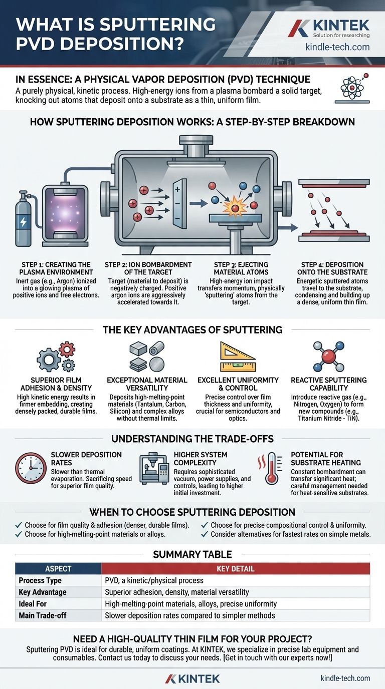
In essence, sputtering deposition is a Physical Vapor Deposition (PVD) technique where a solid source material, known as the "target," is bombarded with high-energy ions from a plasma. This bombardment physically knocks out, or "sputters," atoms from the target's surface. These ejected atoms then travel through a vacuum and deposit onto a substrate, forming an exceptionally thin and uniform film.
Sputtering is not a thermal process of melting and boiling material; it is a purely physical, kinetic process. This fundamental difference is why it excels at producing high-quality films from materials that are difficult or impossible to deposit using other methods.
How Sputtering Deposition Works: A Step-by-Step Breakdown
To understand why sputtering is so effective, it's useful to visualize the process from start to finish within the vacuum chamber.
Step 1: Creating the Plasma Environment
The process begins by introducing an inert gas, most commonly argon (Ar), into a high-vacuum chamber.
A high voltage is then applied, which ionizes the argon gas atoms. This creates a plasma, a glowing state of matter consisting of positive argon ions and free electrons.
Step 2: Ion Bombardment of the Target
The solid material you wish to deposit is set up as the "target" (the cathode). This target is given a negative electrical charge.
The positively charged argon ions in the plasma are aggressively accelerated toward the negatively charged target, striking its surface with immense kinetic energy.
Step 3: Ejecting Material Atoms
When an argon ion collides with the target, it transfers its momentum, much like a cue ball breaking a rack of billiard balls.
If the ion's energy is high enough (typically several times the material's bond energy), it dislodges one or more atoms from the target's surface. This physical ejection is the core "sputtering" action.
Step 4: Deposition onto the Substrate
The sputtered atoms are ejected with significantly more kinetic energy than atoms from thermal evaporation.
These energetic atoms travel in a straight line until they strike the nearby substrate (the object being coated), where they condense and build up, layer by layer, to form a highly uniform and dense thin film.
The Key Advantages of Sputtering
Sputtering is chosen over other deposition methods for several critical reasons, primarily related to film quality and material flexibility.
Superior Film Adhesion and Density
The high kinetic energy of the sputtered atoms means they embed more firmly into the substrate's surface.
This results in superior adhesion and creates films that are more densely packed and durable compared to lower-energy processes.
Exceptional Material Versatility
Because sputtering is a physical rather than a thermal process, it is not limited by a material's melting point.
This allows it to effectively deposit materials with extremely high melting points like tantalum, carbon, and silicon. It also excels at depositing complex alloys and compounds, as the material's composition is accurately transferred from the target to the substrate.
Excellent Uniformity and Control
Sputtering provides exceptional control over film thickness and uniformity across the entire surface of the substrate.
This level of precision is why it is a foundational process in industries like semiconductor manufacturing, where even microscopic inconsistencies can cause device failure.
Reactive Sputtering Capability
By introducing a reactive gas (like nitrogen or oxygen) into the chamber along with the inert gas, you can form new compounds on the substrate.
For example, sputtering a titanium target in the presence of nitrogen gas will create an ultra-hard titanium nitride (TiN) coating, a process known as reactive sputtering.
Understanding the Trade-offs
No single process is perfect for every application. Understanding the limitations of sputtering is crucial for making an informed decision.
Slower Deposition Rates
Generally, sputtering is a slower deposition method compared to techniques like thermal evaporation. The process of physically ejecting atoms one by one is less rapid than boiling a material.
This is the classic trade-off: sacrificing speed for superior film quality.
Higher System Complexity
Sputtering systems require sophisticated vacuum chambers, high-voltage power supplies (DC for conductive targets, RF for insulators), and precise gas flow controls.
This makes the initial equipment investment and operational complexity higher than for simpler deposition methods.
Potential for Substrate Heating
While considered a low-temperature process compared to Chemical Vapor Deposition (CVD), the constant bombardment of energetic atoms can still transfer a significant amount of heat to the substrate.
For extremely heat-sensitive substrates, this energy transfer must be carefully managed to prevent damage.
When to Choose Sputtering Deposition
Your final decision should be driven by the specific requirements of your material and the desired quality of the final film.
- If your primary focus is film quality and adhesion: Choose sputtering. Its high-energy deposition process creates denser, more durable films that bond exceptionally well to the substrate.
- If you are working with high-melting-point materials or alloys: Sputtering is the superior, and often only, viable PVD choice over thermal evaporation.
- If your application demands precise compositional control and uniformity: Sputtering offers the fine-tuned control necessary for complex applications like semiconductors, optics, and data storage media.
- If your goal is the fastest possible deposition rate for simple metals: You might consider thermal evaporation, but you must be prepared to accept the resulting trade-offs in film density and adhesion.
By understanding its principles, you can leverage sputtering to achieve thin films with unparalleled quality and material flexibility.
Summary Table:
| Aspect | Key Detail |
|---|---|
| Process Type | Physical Vapor Deposition (PVD), a kinetic/physical process |
| Key Advantage | Superior film adhesion, density, and material versatility |
| Ideal For | High-melting-point materials, alloys, and applications requiring precise uniformity |
| Main Trade-off | Slower deposition rates compared to simpler methods like thermal evaporation |
Need a high-quality thin film for your project?
Sputtering PVD deposition is ideal for creating durable, uniform coatings on everything from semiconductors to specialized alloys. At KINTEK, we specialize in providing the precise lab equipment and consumables you need to achieve superior results.
Our experts can help you select the right sputtering system for your specific materials and application requirements. Contact us today to discuss how we can support your laboratory's thin film deposition needs.
Get in touch with our experts now!
Visual Guide
Related Products
- RF PECVD System Radio Frequency Plasma-Enhanced Chemical Vapor Deposition RF PECVD
- Inclined Rotary Plasma Enhanced Chemical Vapor Deposition PECVD Equipment Tube Furnace Machine
- Evaporation Boat for Organic Matter
- Vacuum Hot Press Furnace Machine for Lamination and Heating
- Electron Beam Evaporation Coating Oxygen-Free Copper Crucible and Evaporation Boat
People Also Ask
- What is the principle of plasma enhanced chemical vapor deposition? Achieve Low-Temperature Thin Film Deposition
- Why is PECVD environment friendly? Understanding the Eco-Friendly Benefits of Plasma-Enhanced Coating
- How does RF power create plasma? Achieve Stable, High-Density Plasma for Your Applications
- What is an example of PECVD? RF-PECVD for High-Quality Thin Film Deposition
- What are the advantages of PECVD? Enable Low-Temperature, High-Quality Thin-Film Deposition