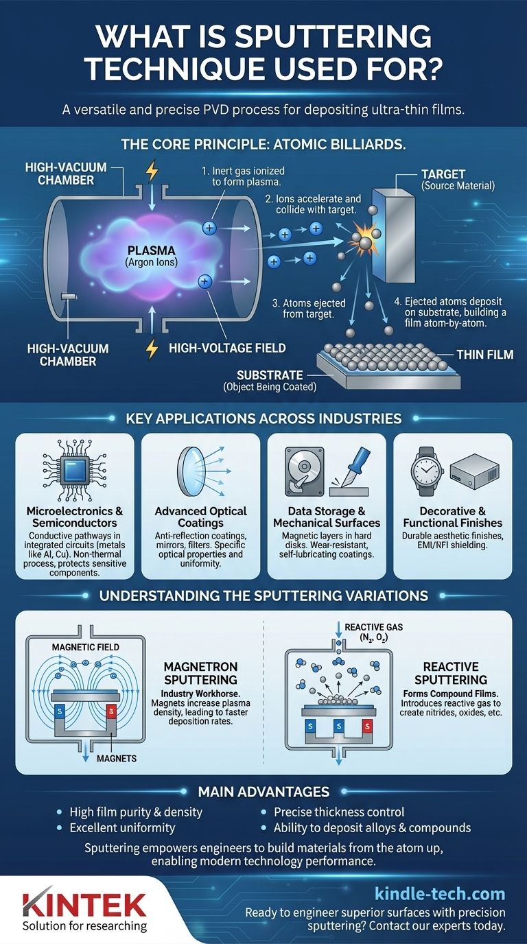
At its core, sputtering is a highly versatile and precise vacuum-based technique used to deposit ultra-thin films of material onto a surface. This physical vapor deposition (PVD) process is fundamental to manufacturing countless modern technologies, from the integrated circuits in your phone to the anti-reflective coatings on your glasses. It works by ejecting atoms from a source material (a "target"), which then travel and condense onto a substrate, forming a new, functional layer.
Sputtering is not merely a coating method; it is a foundational process for engineering surfaces at the atomic level. Its primary use is to create thin films with specific, highly controlled optical, electrical, or mechanical properties that are critical for advanced applications.
How Sputtering Functions as an Atomic-Scale Tool
Sputtering is a physical process, not a chemical one. Understanding this distinction is key to grasping its capabilities.
The Core Principle: Atomic Billiards
The process takes place within a high-vacuum chamber. A high-voltage electric field energizes an inert gas (typically Argon), stripping electrons from the gas atoms and creating a plasma of positively charged ions.
These high-energy ions are then accelerated and directed toward the "target," which is a block of the material you wish to deposit. When the ions collide with the target, they transfer momentum and eject atoms from its surface, a process conceptually similar to a cue ball breaking a rack of billiard balls.
Deposition: Building the Thin Film
The ejected target atoms travel through the vacuum chamber and land on the "substrate"—the object being coated. Because this happens atom-by-atom in a controlled environment, the resulting film is exceptionally uniform, dense, and pure, with a thickness that can be controlled from a few nanometers to several micrometers.
Key Applications Across Industries
The ability to create such precise films makes sputtering indispensable in sectors where material performance is paramount.
Microelectronics and Semiconductors
Sputtering is a cornerstone of semiconductor manufacturing. It is used to deposit the thin layers of metals (like aluminum or copper) that form the conductive pathways in integrated circuits.
Because it is a non-thermal process, it can deposit materials without damaging sensitive underlying electronic components, a critical requirement in microchip fabrication.
Advanced Optical Coatings
The technique is used to create films with specific optical properties. Applications include anti-reflection coatings on lenses, reflective layers on mirrors and architectural glass, and filters that transmit or block specific wavelengths of light.
Data Storage and Mechanical Surfaces
Sputtering was one of the earliest methods used to produce computer hard disks, depositing the magnetic layers that store data.
It is also used to create super-hard, wear-resistant films on cutting tools and self-lubricating coatings on mechanical components, dramatically extending their operational life.
Decorative and Functional Finishes
From the metallic sheen on a watch to EMI/RFI shielding on electronic enclosures, sputtering provides durable and uniform decorative and functional coatings.
Understanding the Sputtering Variations
Not all sputtering is the same. The basic process has been refined to solve specific engineering challenges, leading to several key variations.
Magnetron Sputtering: The Industry Workhorse
The most common industrial method is magnetron sputtering. By placing powerful magnets behind the target, a magnetic field is created that traps electrons near the target's surface.
This significantly increases the efficiency of the gas ionization process, leading to a denser plasma and much faster deposition rates. This innovation made sputtering economically viable for large-scale production.
Reactive Sputtering: Creating New Compounds
In reactive sputtering, a reactive gas like nitrogen or oxygen is intentionally introduced into the vacuum chamber along with the inert gas.
The sputtered metal atoms react with this gas on their way to the substrate, forming compound films like nitrides or oxides. This is how materials like durable titanium nitride (TiN) or insulating silicon dioxide (SiO₂) are created.
Common Limitations and Trade-offs
While powerful, sputtering is not a universal solution. The equipment is complex and requires a high-vacuum environment, representing a significant capital investment.
Deposition rates can be slower than other methods like thermal evaporation, although magnetron sputtering helps mitigate this. The cost and fabrication of the source material targets can also be a factor for certain exotic materials.
Making the Right Choice for Your Goal
Sputtering is chosen when the precision and quality of the thin film are more important than the raw speed of deposition.
- If your primary focus is high-purity, complex electronic films: Sputtering is the definitive choice for creating the precise, multi-layered conductive and dielectric structures required in semiconductors.
- If your primary focus is advanced optical performance: The technique provides superior control over film thickness and uniformity, essential for creating high-performance anti-reflective, reflective, or filtering coatings.
- If your primary focus is superior material properties: Reactive sputtering allows you to engineer compound films with exceptional hardness, resistance, or specific electrical characteristics that don't exist in bulk form.
Ultimately, sputtering empowers engineers to build materials from the atom up, enabling the performance that defines modern technology.
Summary Table:
| Key Aspect | Description |
|---|---|
| Primary Use | Depositing ultra-thin, uniform films of material onto a substrate (surface). |
| Core Principle | A Physical Vapor Deposition (PVD) process using momentum transfer in a vacuum to eject atoms from a target. |
| Key Industries | Microelectronics, Semiconductors, Advanced Optics, Data Storage, Decorative Finishes. |
| Main Advantages | High film purity and density, excellent uniformity, precise thickness control, ability to deposit alloys and compounds. |
| Common Variations | Magnetron Sputtering (high efficiency), Reactive Sputtering (forms compound films like nitrides/oxides). |
Ready to engineer superior surfaces with precision sputtering?
KINTEK specializes in providing advanced lab equipment and consumables for thin-film deposition. Whether you are developing next-generation semiconductors, high-performance optical coatings, or durable protective layers, our expertise and solutions are tailored to meet the exacting demands of modern laboratory research and development.
Contact our experts today to discuss how we can support your specific thin-film application and help you achieve unparalleled material performance.
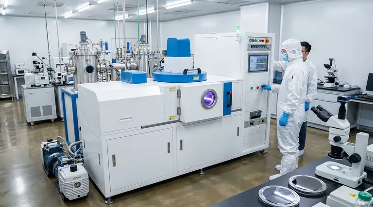
Visual Guide
Related Products
- Spark Plasma Sintering Furnace SPS Furnace
- Vacuum Induction Melting Spinning System Arc Melting Furnace
- Chemical Vapor Deposition CVD Equipment System Chamber Slide PECVD Tube Furnace with Liquid Gasifier PECVD Machine
- Customer Made Versatile CVD Tube Furnace Chemical Vapor Deposition Chamber System Equipment
- Vacuum Cold Mounting Machine for Sample Preparation
People Also Ask
- What are the advantages of CAMI/SPS for W-Cu composite preparation? Reduce cycles from hours to seconds.
- What technical advantages does a Spark Plasma Sintering (SPS) furnace offer for LZP ceramics? Enhance Ionic Conductivity
- What is the process fundamentals of spark plasma sintering? Achieve Rapid, High-Density Material Consolidation
- What is the theory of spark plasma sintering? A Guide to Rapid, Low-Temperature Densification
- Why are Spark Plasma Sintering (SPS) furnaces or hot presses utilized in the preparation of Li3PS4 solid electrolytes?


