The primary advantage of Chemical Vapor Deposition (CVD) over thermal oxidation is its profound versatility. While oxidation is a highly specialized process that grows a single material (silicon dioxide) from a silicon substrate, CVD is a flexible technique that can deposit a vast array of different materials onto nearly any substrate. This makes CVD an indispensable tool for building the complex, multi-layered structures of modern electronics.
The choice between CVD and oxidation is not about which process is universally "better," but about understanding their fundamental purposes. Oxidation grows a high-quality native material by consuming the substrate, while CVD deposits a separate material on top of it.
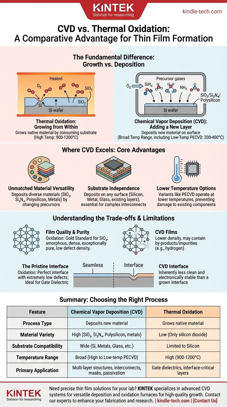
The Fundamental Difference: Growth vs. Deposition
To grasp the advantages of each method, you must first understand their core mechanisms. They are not interchangeable; they are fundamentally different ways of forming a thin film.
Thermal Oxidation: Growing from Within
Thermal oxidation is a growth process. A silicon wafer is heated to a high temperature (typically 900-1200°C) in an environment containing oxygen or water vapor.
The silicon atoms at the surface of the wafer react with the oxygen, consuming the original silicon to form a new layer of silicon dioxide (SiO₂). This process is akin to skin healing—the new layer is formed directly from the underlying material.
Chemical Vapor Deposition: Adding a New Layer
CVD is a deposition process. Precursor gases are introduced into a reaction chamber where they chemically react and decompose, leaving a solid thin film on the surface of the wafer.
This process does not consume the substrate. It is like painting a wall—you are adding an entirely new material on top of the existing surface. This allows for the creation of films that are chemically distinct from the substrate below.
Where CVD Excels: The Core Advantages
The deposition-based nature of CVD gives it several critical advantages over oxidation for a wide range of applications in semiconductor manufacturing.
Unmatched Material Versatility
Oxidation can only create one material: silicon dioxide from a silicon wafer.
CVD, however, can deposit a huge variety of materials by simply changing the precursor gases. This includes dielectrics like silicon dioxide (SiO₂) and silicon nitride (Si₃N₄), semiconductors like polysilicon, and even metals.
Substrate Independence
The oxidation process is entirely dependent on having a silicon substrate to consume. You cannot use it to form an oxide layer on top of a metal line or a nitride film.
CVD has no such limitation. It can deposit a film on silicon, metal, glass, or other previously deposited layers, making it essential for creating the multi-level interconnects in modern chips.
Lower Temperature Options
High-temperature thermal oxidation can damage other components on a partially fabricated chip, such as aluminum interconnects.
While some CVD processes are high-temperature, variants like Plasma-Enhanced CVD (PECVD) can operate at much lower temperatures (e.g., 200-400°C), making them safe for later-stage fabrication steps.
Understanding the Trade-offs
Choosing a process requires acknowledging its limitations. While versatile, CVD films cannot match the unique quality of a thermally grown oxide for its specific purpose.
Film Quality and Purity
For creating silicon dioxide, thermal oxidation is the gold standard. It produces an amorphous, dense, and exceptionally pure film with very low defect density.
CVD-deposited oxides, while very good, often have lower density and can contain by-products from the chemical reaction, such as hydrogen impurities.
The Pristine Interface
This is the most critical distinction. Because thermal oxide is grown from the silicon, the interface between the silicon crystal and the silicon dioxide layer is nearly perfect, with an extremely low number of electronic defects.
The interface created by CVD is simply where a deposited film meets the substrate. It is inherently less clean and electronically stable than a thermally grown interface. For this reason, thermal oxide is the non-negotiable choice for the critical gate dielectric in a transistor.
Making the Right Choice for Your Goal
The correct process is dictated entirely by the specific engineering requirement at each stage of fabrication.
- If your primary focus is creating a high-performance gate dielectric for a transistor: Thermal oxidation is the only choice due to its superior interface and film quality.
- If your primary focus is depositing an insulating layer between metal lines: CVD is the necessary tool, as it can deposit SiO₂ or other dielectrics on top of various materials.
- If your primary focus is creating a hard mask or a final passivation layer: CVD is your only option for depositing a required material like silicon nitride (Si₃N₄).
Ultimately, understanding the fundamental distinction between growing a native film and depositing a foreign one is the key to mastering modern fabrication.
Summary Table:
| Feature | Chemical Vapor Deposition (CVD) | Thermal Oxidation |
|---|---|---|
| Process Type | Deposits new material on substrate | Grows material from substrate |
| Material Variety | High (SiO₂, Si₃N₄, polysilicon, metals) | Low (only silicon dioxide) |
| Substrate Compatibility | Wide (silicon, metals, glass, existing layers) | Limited to silicon substrates |
| Temperature Range | Broad (including low-temp PECVD options) | High (900-1200°C) |
| Primary Application | Multi-layer structures, interconnects, masks | Gate dielectrics, interface-critical layers |
Need precise thin film solutions for your lab? KINTEK specializes in advanced lab equipment and consumables for semiconductor research and development. Whether you require CVD systems for versatile material deposition or oxidation furnaces for high-quality interface growth, our expertise ensures optimal process performance. Contact our experts today to discuss how our solutions can enhance your fabrication capabilities and accelerate your research.
Visual Guide
Related Products
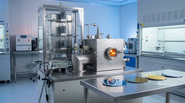
- Chemical Vapor Deposition CVD Equipment System Chamber Slide PECVD Tube Furnace with Liquid Gasifier PECVD Machine
- RF PECVD System Radio Frequency Plasma-Enhanced Chemical Vapor Deposition RF PECVD
- Microwave Plasma Chemical Vapor Deposition MPCVD Machine System Reactor for Lab and Diamond Growth
- Customer Made Versatile CVD Tube Furnace Chemical Vapor Deposition Chamber System Equipment
- 915MHz MPCVD Diamond Machine Microwave Plasma Chemical Vapor Deposition System Reactor
People Also Ask
- What is plasma enhanced chemical vapor deposition PECVD equipment? A Guide to Low-Temperature Thin Film Deposition
- How expensive is chemical vapor deposition? Understanding the True Cost of High-Performance Coating
- What types of substrates are used in CVD to facilitate graphene films? Optimize Graphene Growth with the Right Catalyst
- How are carbon nanotubes grown? Master Scalable Production with Chemical Vapor Deposition
- What are the advantages of chemical vapor deposition? Achieve Superior Thin Films for Your Lab


